Light-emitting device

a light-emitting device and light-emitting technology, applied in the direction of organic semiconductor devices, instruments, optics, etc., can solve the problems of reduced yield, increased cost, and limitation in the mounting method of ic formed by a single crystalline silicon wafer on a glass substrate, and achieve the effect of reducing cos

Inactive Publication Date: 2005-01-20
SEMICON ENERGY LAB CO LTD
View PDF31 Cites 198 Cited by
  • Summary
  • Abstract
  • Description
  • Claims
  • Application Information

AI Technical Summary

Benefits of technology

[0009] In view of the foregoing, it is an object of the present invention to realize system on panel without complicating the pr...

Problems solved by technology

Therefore, it has been considered that there is a limitation in a method of mounting IC formed by a single crystalline silicon wafer on a glass substrate.
However, there are problems that the process becomes complicated due to crystallization of a semiconductor film, yields becomes reduced, and the cost becomes increased compared to the case of using an amorphous semiconductor film.
Accordingly, throughput in the process of crystallization is declined and the crystallinity by the edge-neighborhood of a laser beam is varied due to that the longitudinal length of the lase...

Method used


Image

  • Light-emitting device
  • Light-emitting device
  • Light-emitting device

Examples


example 1

[0101] A semiamorphous TFT that can be used in the present invention can be either n-type or p-type. The semiamorphous TFT is preferably n-type since an n-type semiamorphous TFT has high mobility and is suitable for using as a pixel of a light-emitting device. In this example, a cross-sectional structure of a pixel is explained using an example of an n-type drive TFT.

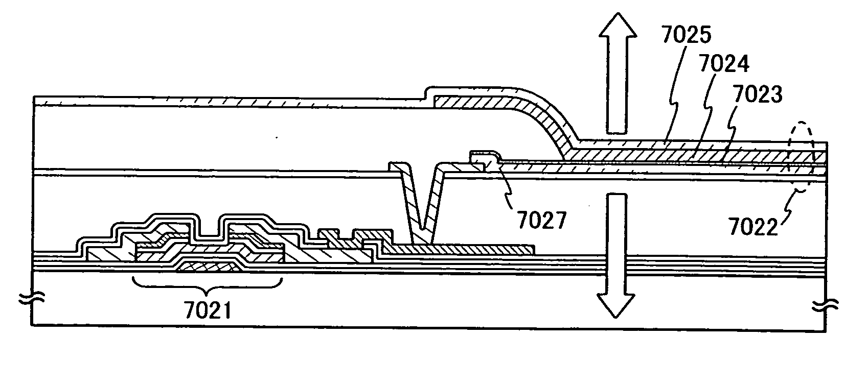
[0102]FIG. 11B is a cross-sectional view of a pixel used in the case that a drive TFT 7001 is n-type, and light generated in a light-emitting element 7002 emits passing through an anode 7005. In FIGS. 11A and 11B, a cathode 7003 of the light-emitting element 7002 and the drive TFT 7001 are electrically connected each other. An electroluminescent layer 7004 and an anode 7005 are sequentially stacked over the cathode 7003. As the cathode 7003, a known material can be used as long as it is a conductive film having small work function and reflects light. For example, Ca, Al, CaF, MgAg, AlLi, or the like is preferably used....

example 2

[0112] In this example, an example of variation of a pixel using a semiamorphous TFT included in a light-emitting device according to the invention is explained.

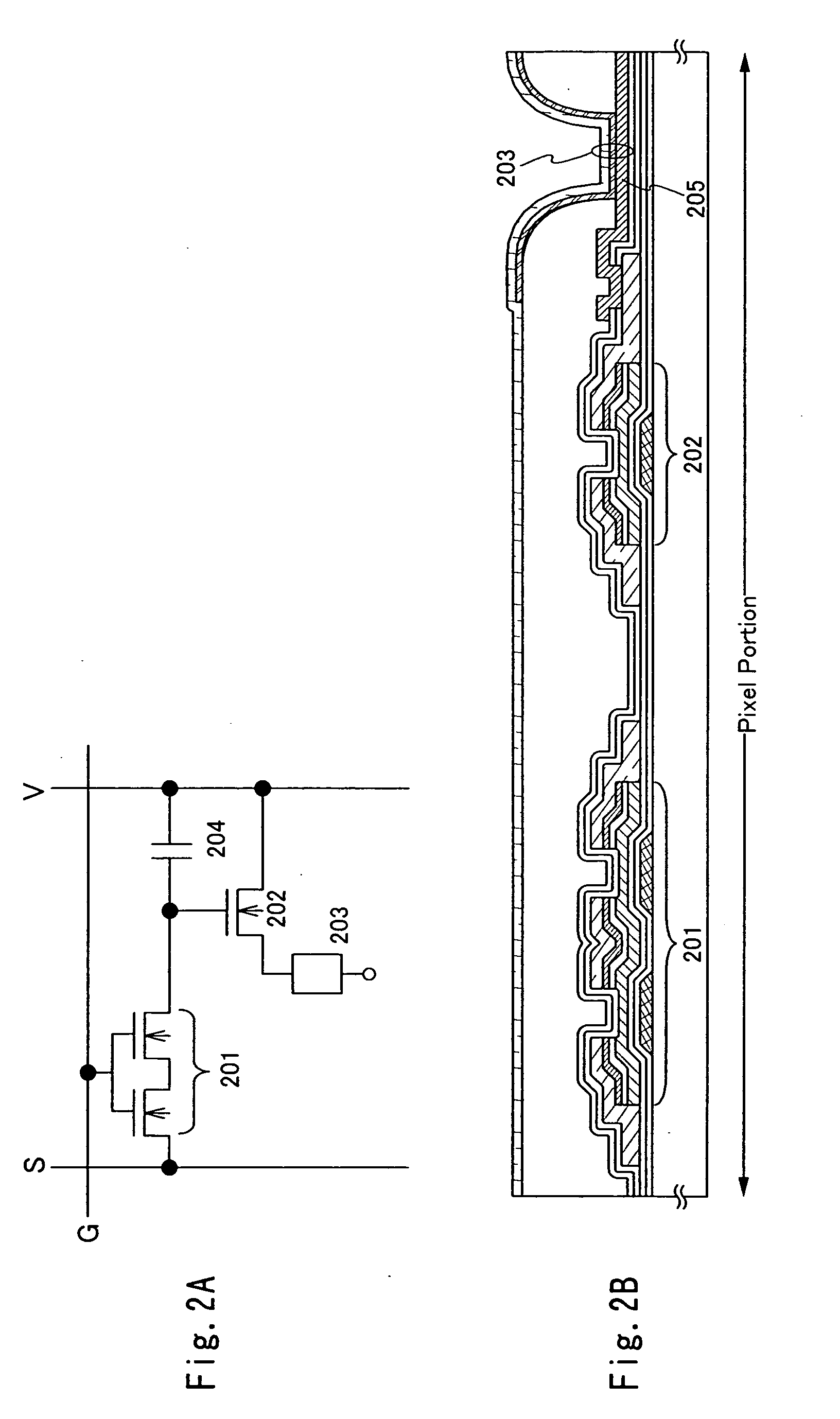
[0113]FIG. 12A shows an embodiment of a pixel according to this example. A pixel shown in FIG. 12A comprising a light-emitting element 901, a switching TFT 902 used as a switching element for controlling the input of a video signal to the pixel, a drive TFT 903 for controlling a current value flowing through the light-emitting element 901, and a current control TFT 904 for determining to supply current or not to the light-emitting element 901. Moreover, a capacitor element 905 for holding electric potential of a video signal may be provided to the pixel as in Embodiment.

[0114] The switching TFT 902, the drive TFT 903, and the current control TFT 904, which may be either n-type or p-type, have the same polarity. The drive TFT 903 operates in a saturation region and the current control TFT 904 operates in a linear region.

[0...

example 3

[0126] In this example, one embodiment of a semiamorphous TFT included in a light-emitting device according to the invention is explained.

[0127]FIG. 13A is a top view of a semiamorphous TFT. FIG. 13B is a cross-sectional view of FIG. 13A taken along line A-A′. Reference numeral 1301 denotes a gate wiring a part of which serves as a gate electrode. The gate wiring 1301 overlaps with a first semiconductor film 1303 formed by semiamorphous semiconductor via a gate insulating film 1302. Second semiconductor films 1304a, 1304b are formed on the first semiconductor film 1303. Third semiconductor films 1305a, 1305b imparting one conductivity type are formed on the second semiconductor films 1304a, 1304b. Each reference numeral 1306, 1307 denotes wiring formed on the third semiconductor films 1305a, 1305b.

[0128] In a semiamorphous TFT shown in FIGS. 13A and 13B, a channel length can be kept constantly by spacing out the interval between the third semiconductor film 1305a and the third sem...


PUM


Abstract

According to present invention, system on panel without complicating the process of TFT can be realized, and a light-emitting device that can be formed by lower cost than that of the conventional light-emitting device can be provided. A light-emitting device is provided in which a pixel portion is provided with a pixel including a light-emitting element and a TFT for controlling supply of current to the light-emitting element; a TFT included in a drive circuit and a TFT for controlling supply of current to the light-emitting element include a gate electrode, a gate insulating film formed over the gate electrode, a first semiconductor film, which overlaps with the gate electrode via the gate insulating film, a pair of second semiconductor films formed over the first semiconductor film; the pair of second semiconductor films are doped with an impurity to have one conductivity type; and the first semiconductor film is formed by semiamorphous semiconductor.

Description

BACKGROUND OF THE INVENTION [0001] 1. Field of the Invention [0002] This invention relates to a light-emitting device using a thin film transistor for a drive circuit and a pixel portion. [0003] 2. Related Art [0004] In a semiconductor display device formed by using a glass substrate at low cost, the required area for the periphery of a pixel portion (a frame region) for mounting is increased with the increase of screen resolution. Accordingly, the miniaturization of the semiconductor display device tends to be prevented. Therefore, it has been considered that there is a limitation in a method of mounting IC formed by a single crystalline silicon wafer on a glass substrate. Hence, a technique of forming integrally an integrated circuit including a drive circuit over one substrate with a pixel portion, that is, so-called system on panel, has been attracted attention. [0005] A thin film transistor formed by a polycrystalline semiconductor film (polycrystalline TFT) has advantages that...

Claims


Application Information

Patent Timeline
IPC IPC(8): G02F1/136H01L21/336H01L27/12H01L27/32H01L29/786H05B44/00
CPCH01L27/12H01L27/3244H01L29/78669H01L2251/5323H01L29/78678H01L29/66757H10K59/12H10K2102/3031H01L29/458
Inventor YAMAZAKI, SHUNPEI
Owner SEMICON ENERGY LAB CO LTD
Why Eureka
Try Eureka