High efficiency silicon light emitting device and modulator

a light-emitting device, high-efficiency technology, applied in semiconductor devices, instruments, optics, etc., can solve the problems of inability to integrate leds into silicon devices, low conversion efficiency of silicon leds, and inability to meet the requirements of silicon devices

Inactive Publication Date: 2005-01-27
UNISEARCH LTD
View PDF12 Cites 39 Cited by
  • Summary
  • Abstract
  • Description
  • Claims
  • Application Information

AI Technical Summary

Benefits of technology

The light emitting portion of the device of the first aspect of the present invention preferably comprises a thin layer which is thin enough for quantum confinement effects to occur. For example the thin layer may comprise a quantum well. In such embodiments, the means for applying the electric field is preferably arranged such that the electric field is applied across the thin layer substantially normal to a plane defined by the layer. In such an orientation the electric field enables significant quantum confined Stark effect modulation of absorption and emission properties of the thin silicon layer, thus enabling modulation of peak emission wavelength and emission intensity at a given wavelength. However, modulation of the light emission characteristics of the light emitting portion may also be achieved by application of an electric field across the light emitting portion in a direction other than substantially normal to the plane. The thin layer may comprise a crystalline silicon layer comprising the quantum well.
According to a thirteenth aspect, the present invention provides a method of modulating light, the method comprising the steps of: positioning a thin layer of silicon in the path of the light, the silicon layer exhibiting quantum confinement effects; and applying an electric field across the thin silicon layer so as to alter the bandgap of the silicon layer by way of the quantum confined Stark effect, thus controlling whether light is absorbed by the silicon layer or transmitted through the silicon layer.

Problems solved by technology

However, the use of such materials prevents integration of LEDs into silicon devices.
While attempts have been made in the past to manufacture silicon LEDs, the conversion efficiency of silicon LEDs has, for most applications, been unacceptably low.

Method used


Image

  • High efficiency silicon light emitting device and modulator
  • High efficiency silicon light emitting device and modulator
  • High efficiency silicon light emitting device and modulator

Examples


Embodiment Construction

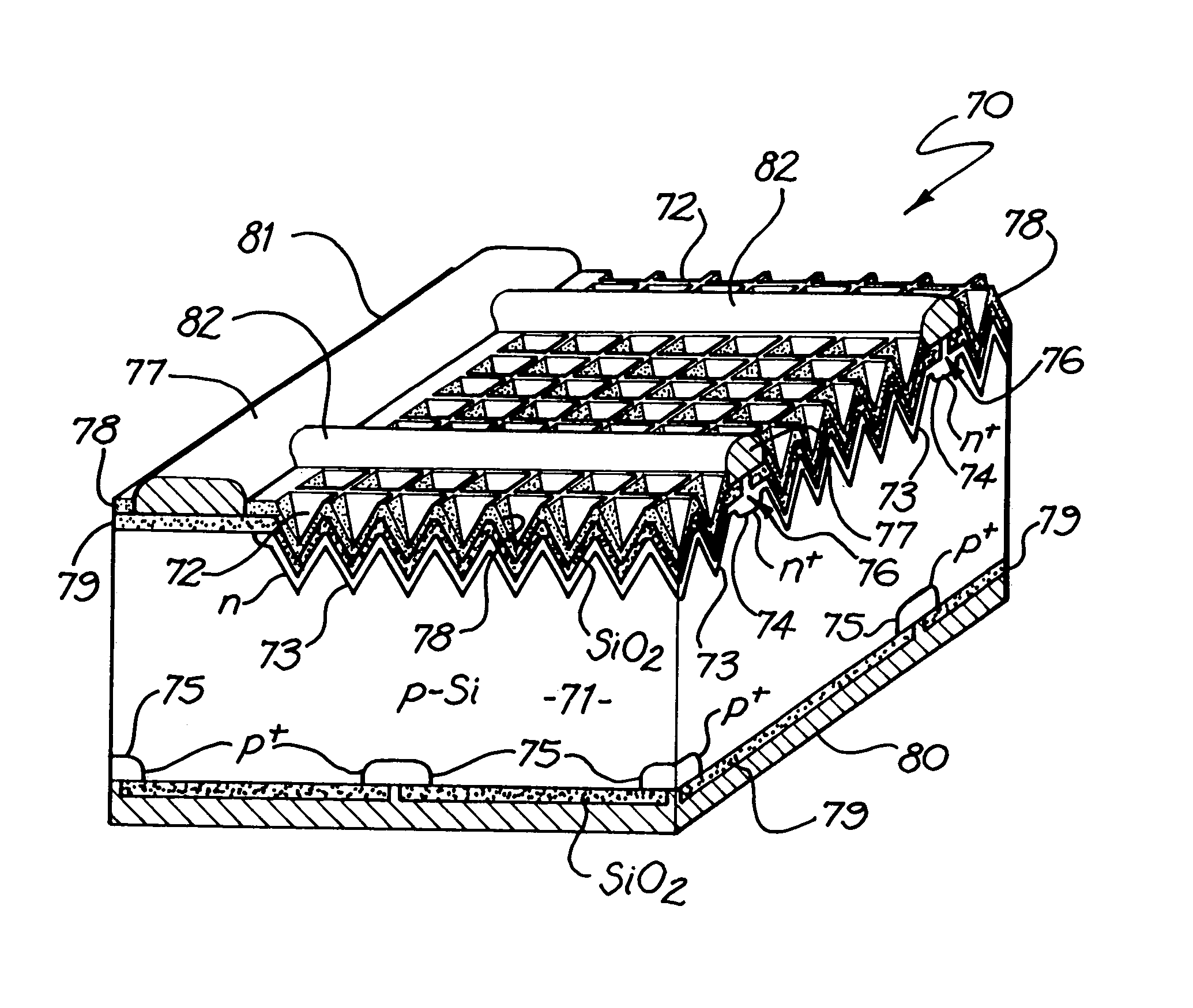
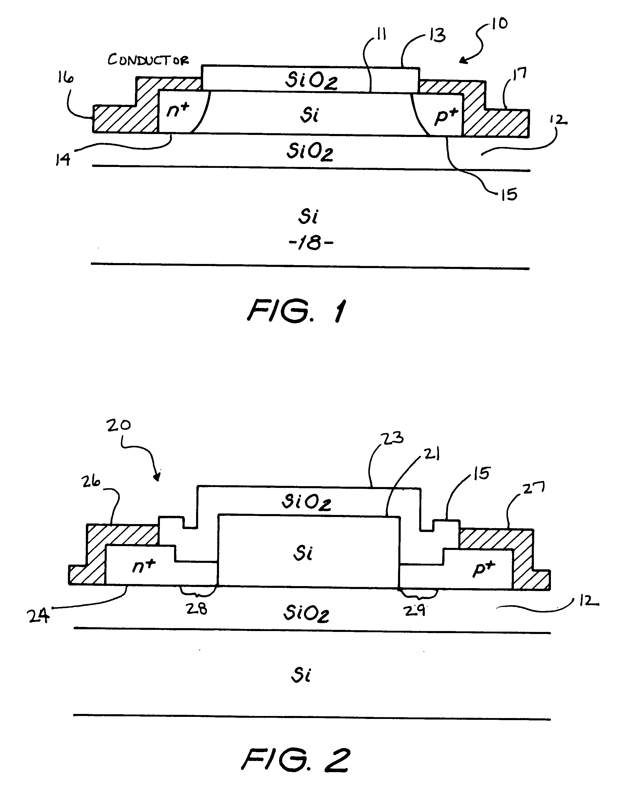
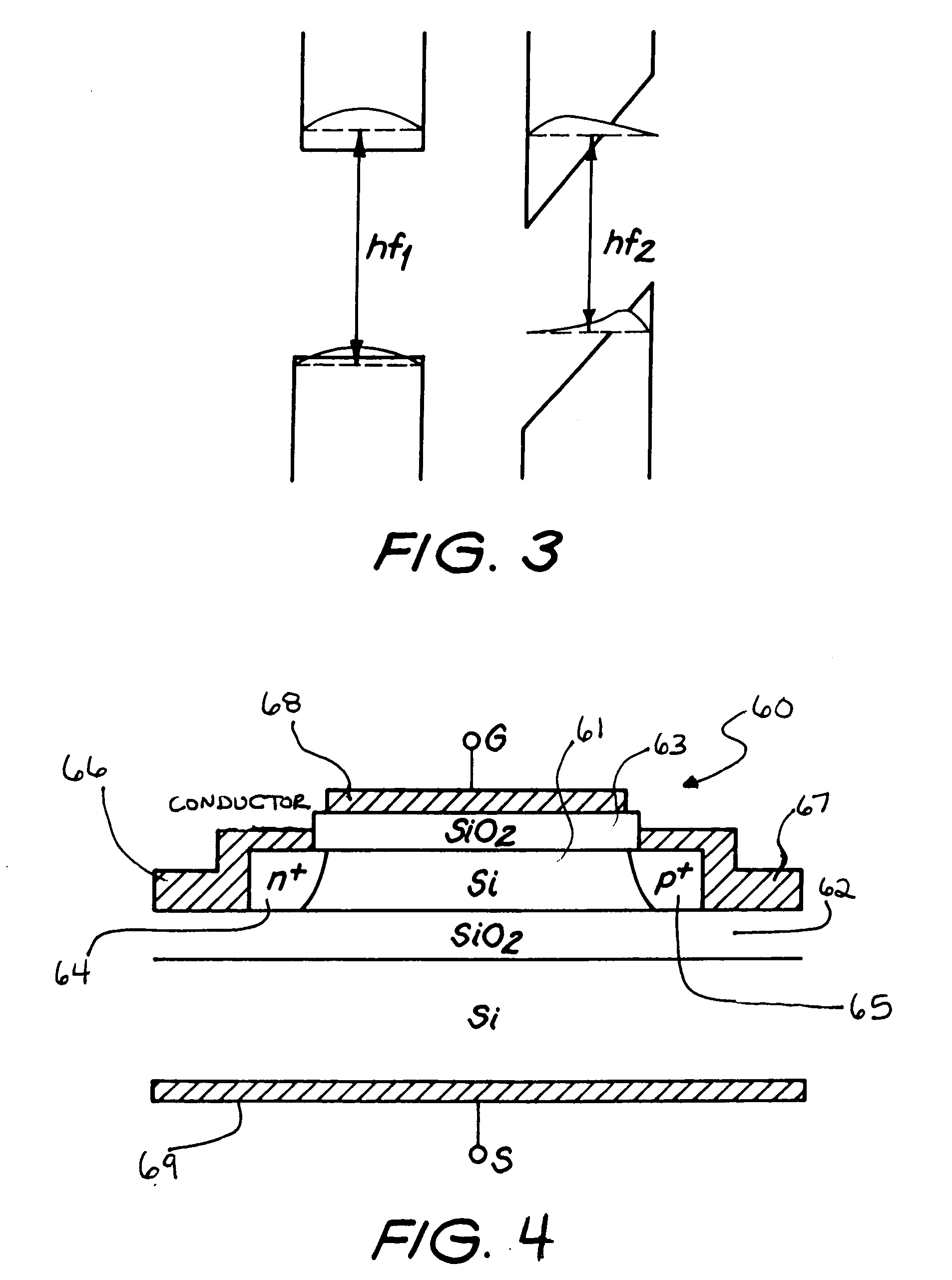
An edge emitting silicon device 10 in accordance with the present invention is shown in FIG. 1. This device makes use of a buried dielectric silicon oxide layer 12 that is an easily obtainable feature when using silicon-on-insulator (SOI) technology. The advantage of this approach is the small device cross sections that are possible, the excellent light confinement prospects possible due to the high refractive index step between the silicon layer 11 and the dielectric layers 12 and 13, generally silicon dioxide, and the suitability for incorporation into standard silicon integrated circuits.

If the top silicon layer 11 is less than about 200 nm thick, as is normally the case for SOI technology, only a single optical waveguide mode can be supported by the layer 11 shown in FIG. 1 in the longitudinal direction into the page (ie normal to the page). Modern lithographic methods allow similar control over lateral dimensions. Minority carrier diffusion lengths in the n+ doped region 14 ...


PUM

PropertyMeasurementUnit
thicknessaaaaaaaaaa
thicknessaaaaaaaaaa
quantum efficiencyaaaaaaaaaa

Abstract

The present invention provides a high performance silicon light emitting device. A method and device providing both emission and modulation from a single device is provided, with modulation of the emission characteristics being achieved by application of an electric field across the device, so as to induce quantum confined Stark effects, Franz-Keldysh effects or the like.

Description

TECHNICAL FIELD The present invention relates to high efficiency silicon light emitting devices such as diodes, and to a method of designing and operating such devices. BACKGROUND ART Light emitting diodes (LEDs) are an extremely common electronic device with a wide range of applications, including displays, short distance communications over fibres, opto-couplers, indicators and infrared wireless communication (including television remote controls and free space data links). LEDs typically comprise a light-emitting gallium arsenide pn junction (which emits based on direct band-to-band transitions) or may comprise GaAs1-xPx, with an isoelectronic dopant such as nitrogen (which emits based on impurity states in the bandgap). GaAs LEDs have been found to offer acceptable quantum efficiencies, approaching 1%, while the use of nitrogen as an isoelectronic dopant in a GaAs1-xPx LED can improve the quantum efficiency of the LED to over 1%. The materials of a LED may also be chosen in o...

Claims


Application Information

Patent Timeline
Patent Type & Authority Applications(United States)
IPC IPC(8): G02F1/015H01L33/34G02F1/017
CPCG02F1/015H01L33/34G02F2202/105
Inventor GREEN, MARTIN ANDREWZHAO, JIANHUA
Owner UNISEARCH LTD
Why Eureka
Try Eureka