Method of forming redistribution bump and semiconductor chip and mount structure fabricated using the same

Active Publication Date: 2005-01-27
SAMSUNG ELECTRONICS CO LTD
View PDF4 Cites 37 Cited by
  • Summary
  • Abstract
  • Description
  • Claims
  • Application Information

AI Technical Summary

Benefits of technology

[0014] The present invention provides a method of forming a bump to simplify an assembly of a semiconductor chip and to minimize a pad area inside the chip

Problems solved by technology

Additionally, the rough upper portion of the bump hampers the bonding process, and chip size is inevitably big due to the formation of the bump 13 on the Al

Method used


Image

  • Method of forming redistribution bump and semiconductor chip and mount structure fabricated using the same
  • Method of forming redistribution bump and semiconductor chip and mount structure fabricated using the same
  • Method of forming redistribution bump and semiconductor chip and mount structure fabricated using the same

Examples


first embodiment

[0028] A method of forming a redistribution bump according to the present invention will be explained with reference to FIGS. 6 through 12.

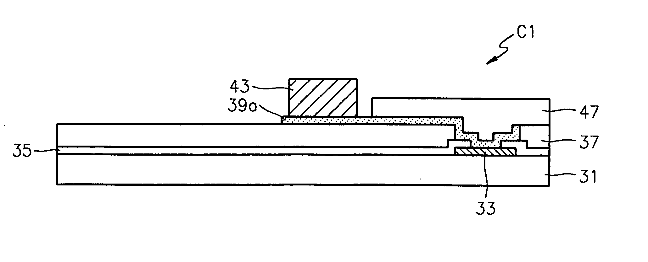
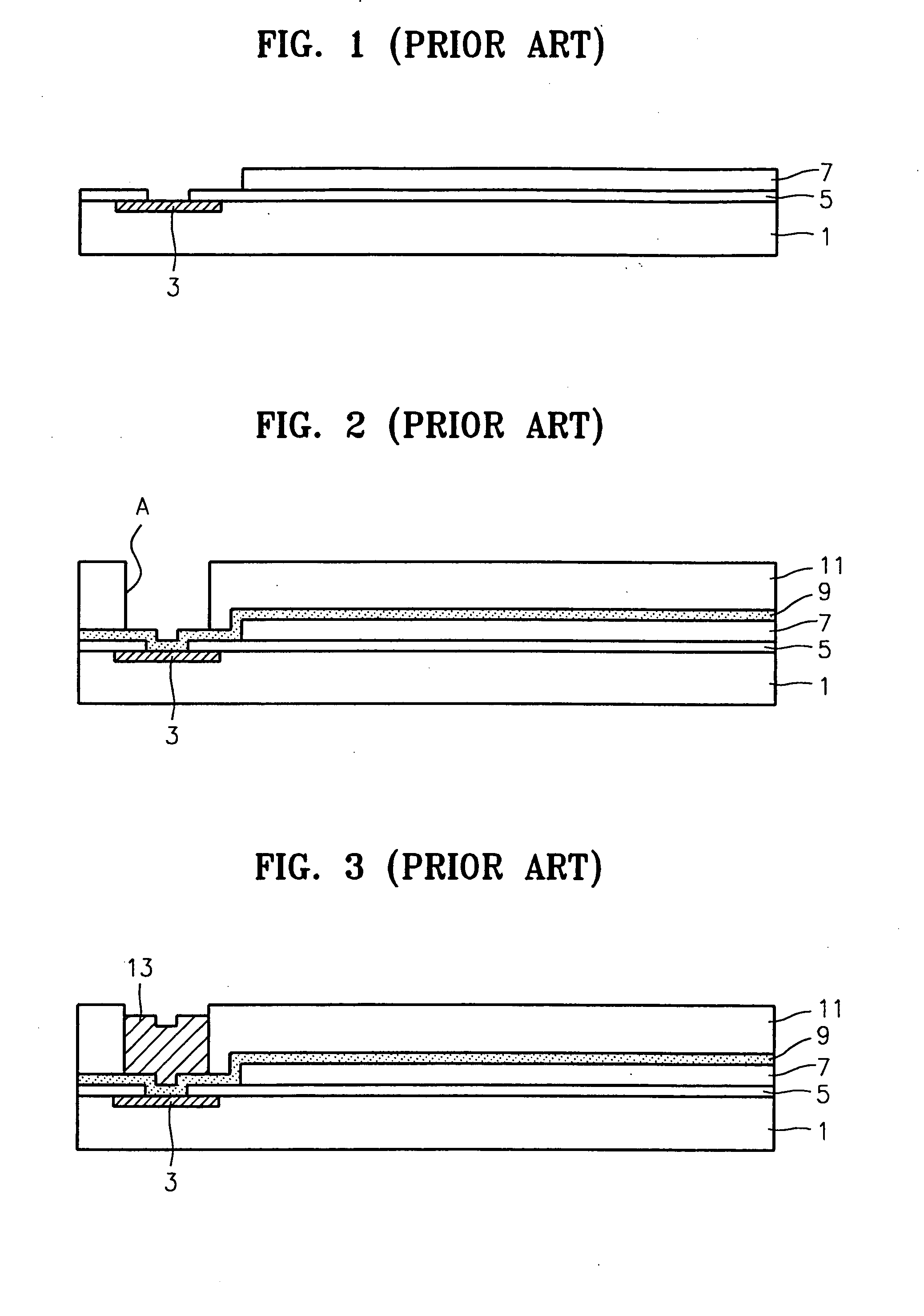
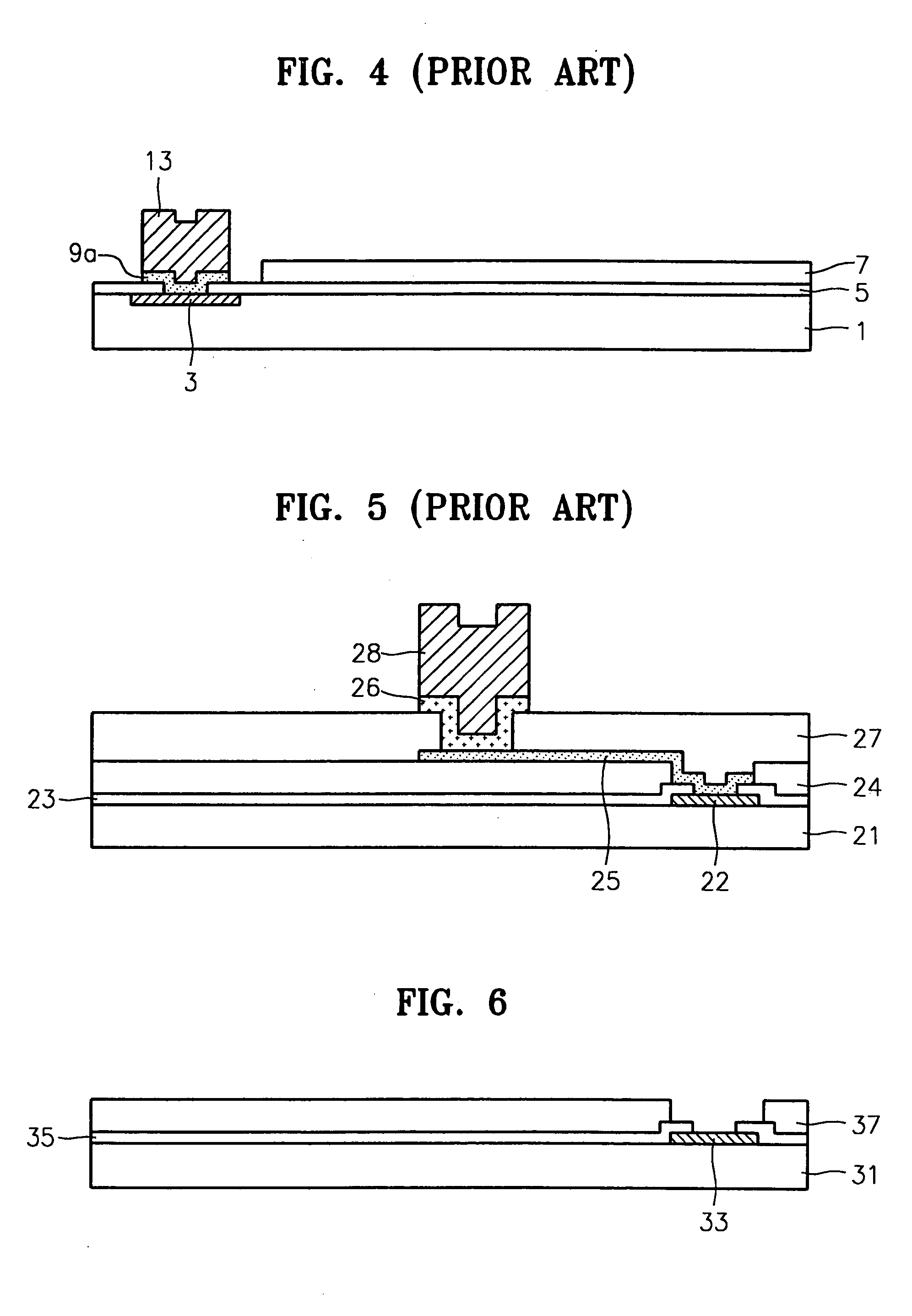
[0029] Referring to FIG. 6, a first passivation film 35 is applied onto an upper portion of a wafer-state chip 31 in which a plurality of semiconductor devices are formed. The upper portion of an Al pad 33, to transmit signals between the semiconductor device and an external electronic device, is exposed by partially etching the first passivation film 35. The first passivation film 35 may comprise a silicon oxide and nitride film. The Al pad 33 may be exposed by a photolithography and etching process. A second passivation film 37, such as polyimide, may be formed over the first passivation film 35 and the Al pad 33 via spin coating. The second passivation film 37 is patterned to expose a portion of the Al pad 33. The second passivation film 37 may comprise, for example, polyetherimide, epoxy, or silicon resin.

[0030] In the embodiment in FIG. 7, ...

second embodiment

[0040] An explanation on the second embodiment will follow one on bump formation in FIGS. 6 through 8. In one embodiment of the present embodiment, the first photoresist pattern 41 used in forming the bump 43 is removed by ashing and stripping as shown in FIG. 13.

[0041] Referring to FIG. 14, a new photoresist pattern 44 is formed a predetermined width from an opening of the first passivation film 35 in the Al pad 33 to the bump 43. The redistribution metal line 39a remains as presented in FIG. 15 by etching the metal layer 39 while using the photoresist pattern 44 as an etching mask.

[0042] After removing the photoresist pattern 44, a chip structure C2 is obtained as shown in FIG. 16 by forming the third passivation film 47 as explained in FIG. 12.

[0043] Although the second photoresist pattern 41 a is formed by additionally exposing the first photoresist pattern 41 in the first embodiment, the new photoresist pattern 44 is formed after removing the first photoresist pattern 41 in t...


PUM


Abstract

Provided are a method of forming a bump whose upper surface is substantially flat and whose area can be enlarged in a uniform pad pitch to simplify mounting a liquid crystal display drive IC (LDI) and a semiconductor chip and a mount structure using the method to minimize a pad area inside the chip. Thus, the pad area on an edge of a conventional chip is minimized and the bump is formed in a substantially flat location inside the chip and an electrical connection between the pad and the bump is performed by a redistribution metal line.

Description

BACKGROUND OF THE INVENTION [0001] This application claims the priority of Korean Patent Application No. 2003-50496, filed on Jul. 23, 2003, in the Korean Intellectual Property Office, the disclosure of which is incorporated herein in its entirety by reference. [0002] 1. Field of the Invention [0003] The present invention relates to a semiconductor chip and a mount structure, and more particularly, to a liquid crystal display drive IC (LDI) chip and the mount structure in which the chip is connected to an external electronic device by a bump. [0004] 2. Description of the Related Art [0005] A liquid crystal display (LCD) is a flat-panel display having the excellent characteristics of thinness, light-weight, and low power consumption. In addition, the LCD also has such characteristics of high resolution, high color display, and high definition. [0006] As is well known, the LCD is made up of a liquid crystal panel (LCP) having liquid crystal injected between two substrates (an array an...

Claims


Application Information

Patent Timeline
IPC IPC(8): H01L21/44H01L21/60H01L23/31H01L23/485
CPCH01L23/3114H01L24/11H01L2924/07802H01L24/12H01L24/16H01L2224/0231H01L2224/13099H01L2924/01013H01L2924/01022H01L2924/01029H01L2924/01046H01L2924/01047H01L2924/01074H01L2924/01075H01L2924/01078H01L2924/01079H01L2924/01082H01L2924/01006H01L2924/01023H01L2924/01024H01L2924/01033H01L2924/014H01L2224/0401H01L2924/00H01L2224/05124H01L2224/05144H01L2224/05147H01L2224/05155H01L2224/05164H01L2224/05166H01L2224/05171H01L2224/05644H01L2224/05647H01L2224/05655H01L2224/05664H01L2224/05666H01L2224/05671H01L2224/02313H01L2224/0236H01L2224/83851H01L24/13H01L24/05H01L24/03H01L2924/0001H01L2224/05548H01L2224/13024H01L24/02H01L2924/00014H01L2924/013H01L2224/02H01L21/60
Inventor KWON, YONG-HWANKANG, SA-YOONLEE, CHUNG-SUN
Owner SAMSUNG ELECTRONICS CO LTD
Why Eureka
Try Eureka