Semiconductor device, method of fabricating same, and, electrooptical device
a semiconductor and thin-film technology, applied in semiconductor devices, coatings, instruments, etc., can solve problems such as difficult formation of thin-film transistors, and achieve the effect of suppressing drawbacks
- Summary
- Abstract
- Description
- Claims
- Application Information
AI Technical Summary
Benefits of technology
Problems solved by technology
Method used
Image

Examples
example 2
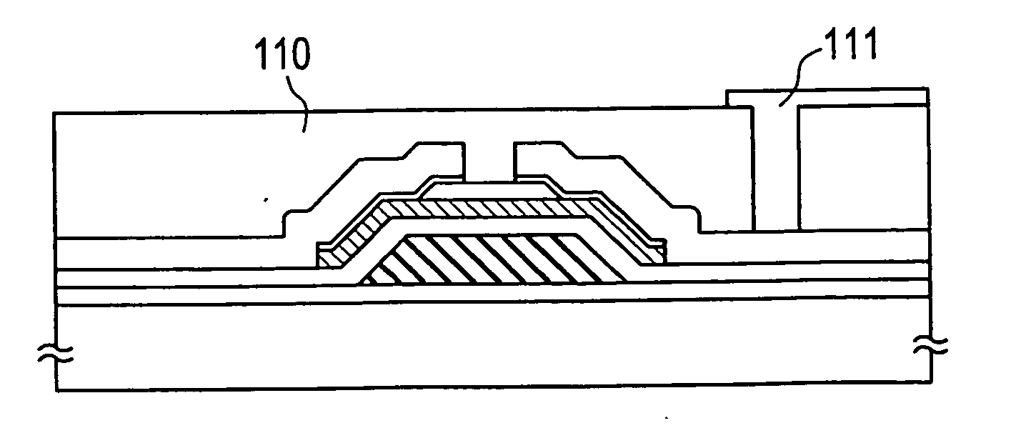
The present example shows a case in which an active matrix liquid crystal display is fabricated, using the thin-film transistors described in Example 1. The liquid crystal electrooptical device described in the present example is shown in FIG. 3 in cross section.
In FIG. 3, PET films 301 and 302 having a thickness of 100 μm form a pair of substrates. An acrylic resin layer 303 acts as a planarizing layer. Indicated by 306 are pixel electrodes. In FIG. 3, only the structure corresponding to two pixels is shown.
Indicated by 304 is a counter electrode. Orientation films 307 and 308 orient a liquid crystal 309 which can be a twisted-nematic (TN) liquid crystal, supertwisted-nematic (STN) liquid crystal, or a ferroelectric liquid crystal. Generally, a TN liquid crystal is employed. The thickness of the liquid crystal layer is several micrometers to about 10 μm.
Thin-film transistors (TFTs) 305 are connected with the pixel electrodes 306. Electric charge going in and out of the pixel...
example 3
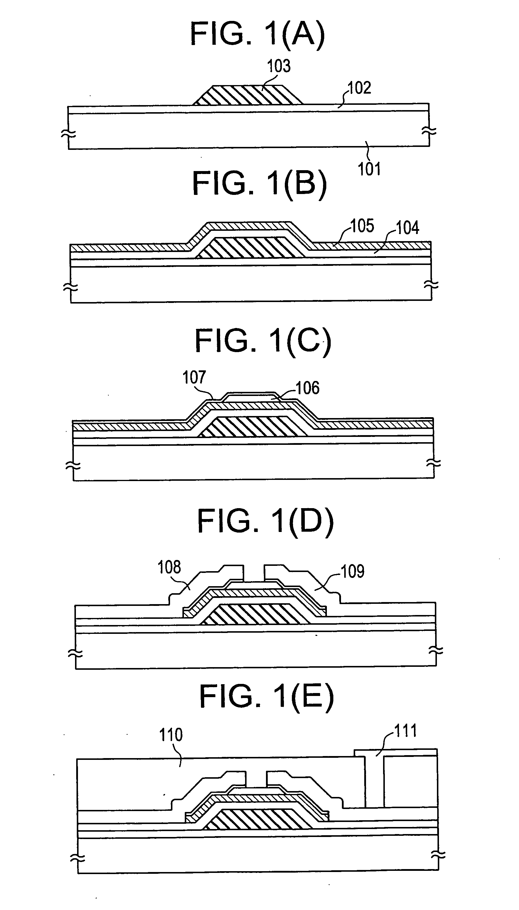
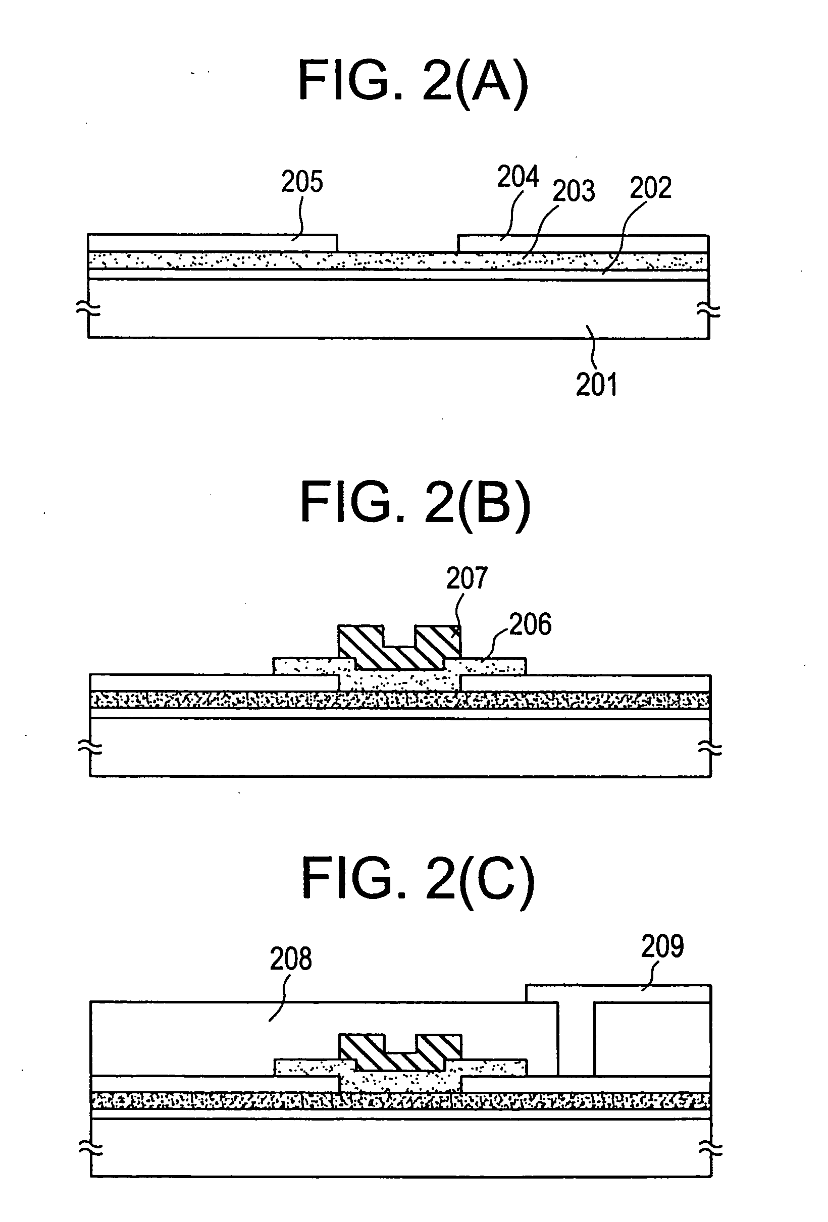
The present example shows an example in which coplanar thin-film transistors used for an active matrix liquid crystal display are fabricated. The process sequence for fabricating the thin-film transistors of the present example is shown in FIG. 2. First, a PET film 201 having a thickness of 100 μm is prepared as a filmy organic resin substrate. The film is heated-treated at 180° C. to promote degassing from the PET film 201. A layer of an acrylic resin 202 is formed on the surface of the film. In this example, an ethyl ester of acrylic acid is used as the acrylic resin.
Then, a substantially intrinsic (I-type) semiconductor layer 203 in which a channel formation region is formed is grown by plasma-assisted CVD under the following conditions:
film formation temperature 160° C.(at which the substrate is heated):reaction pressure: 0.5 torrRF power (13.56 MHz): 20 mW / cm2reactant gas:SiH4
In this example, a parallel-plate plasma-CVD machine is used to grow the film.
Then, an n-type ...
example 4
The present example is similar to the structure of Example 1 or 2 except that the semiconductor layer is made of a microcrystalline semiconductor film. First, a substantially intrinsic semiconductor layer is grown as the microcrystalline semiconductor layer under the following conditions:
film formation temperature 160° C.(at which the substrate is heated):reaction pressure: 0.5 torrRF power (13.56 MHz): 150 mW / cm2reactant gases:SiH4 / H2 = 1 / 30
In this example, a parallel-plate plasma-CVD machine is used to grow the film.
The conditions under which an n-type microcrystalline silicon film is grown are described below. Also in this case, a parallel-plate plasma-CVD machine is used.
film formation temperature 160° C.(at which the substrate is heated):reaction pressure: 0.5 torrRF power (13.56 MHz): 150 mW / cm2reactant gases:B2H6 / SiH4 = 1 / 100
Generally, a microcrystalline silicon film can be obtained by supplying power of 100 to 200 mW / cm2. In the case of the I-type semiconductor lay...
PUM
| Property | Measurement | Unit |
|---|---|---|
| thickness | aaaaa | aaaaa |
| diameters | aaaaa | aaaaa |
| temperature | aaaaa | aaaaa |
Abstract
Description
Claims
Application Information
 - R&D
- Intellectual Property
- Life Sciences
- Materials
- Tech Scout
- Unparalleled Data Quality
- Higher Quality Content
- 60% Fewer Hallucinations
Browse by: Latest US Patents, China's latest patents, Technical Efficacy Thesaurus, Application Domain, Technology Topic, Popular Technical Reports.
© 2025 PatSnap. All rights reserved.Legal|Privacy policy|Modern Slavery Act Transparency Statement|Sitemap|About US| Contact US: help@patsnap.com