Semiconductor device and method of manufacturing the same

a semiconductor and semiconductor technology, applied in semiconductor devices, semiconductor/solid-state device details, capacitors, etc., can solve the problem of difficult removal of sidewall polymers, and achieve the effect of preventing a decrease in the thickness of layers and efficiently forming a wiring structur

Inactive Publication Date: 2005-01-27
SEIKO EPSON CORP
View PDF1 Cites 5 Cited by
  • Summary
  • Abstract
  • Description
  • Claims
  • Application Information

AI Technical Summary

Benefits of technology

[0013] According to the above-described semiconductor device, the protection film formed on the second capacitor electrode, the first hard mask member pattern and the second hard mask member pattern prevents a decrease in the thickness of layers formed on the second capacitor electrode. Moreover, the contact holes which have different depths are stably provided by disposing the protection film formed on the second capacitor electrode, even when these holes are formed simultaneously.
[0014] In the semiconductor device, a plug wiring member pr...

Problems solved by technology

The sidewall polymer is difficult to remove even by c...

Method used


Image

  • Semiconductor device and method of manufacturing the same
  • Semiconductor device and method of manufacturing the same
  • Semiconductor device and method of manufacturing the same

Examples


Embodiment Construction

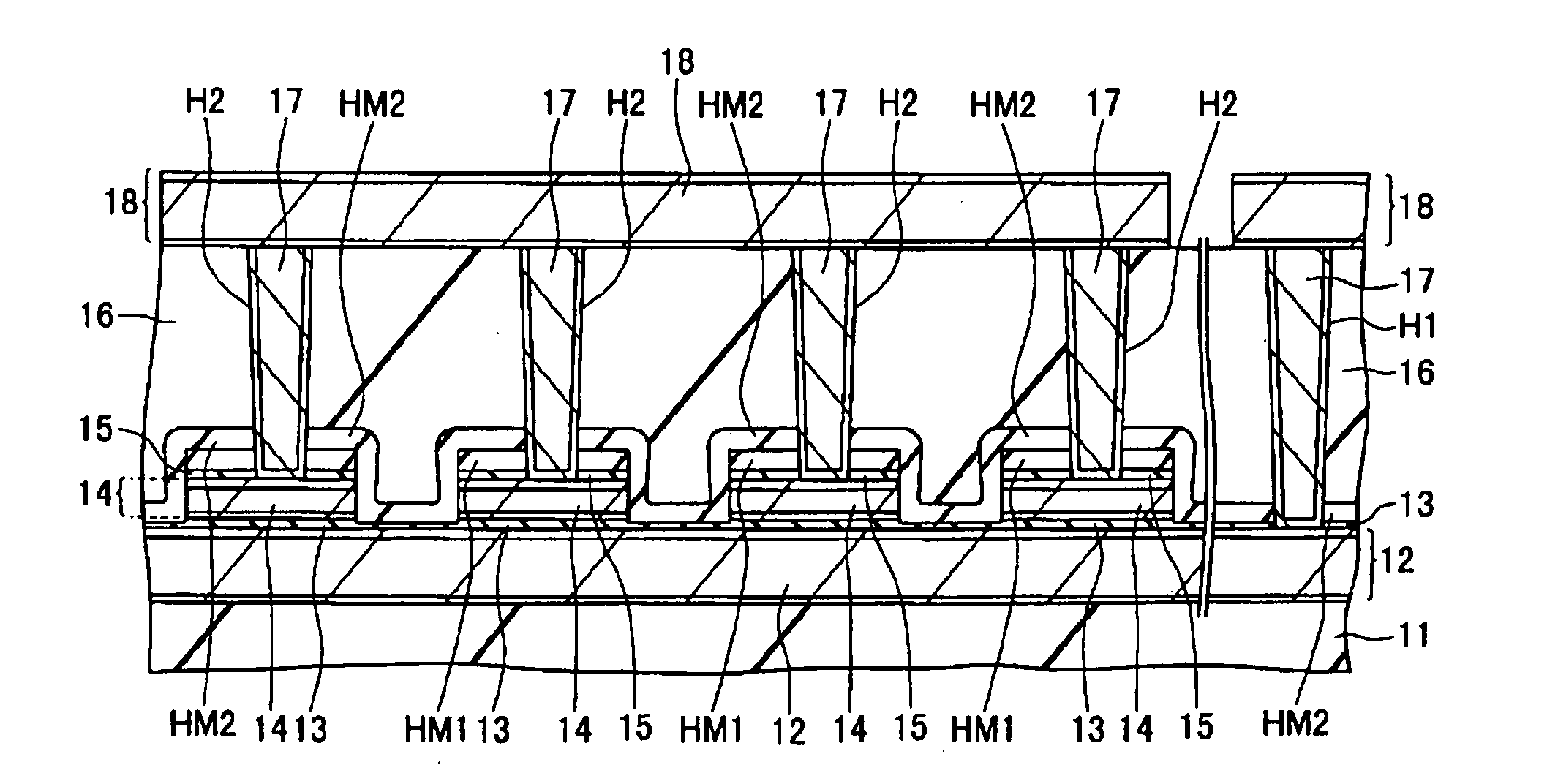
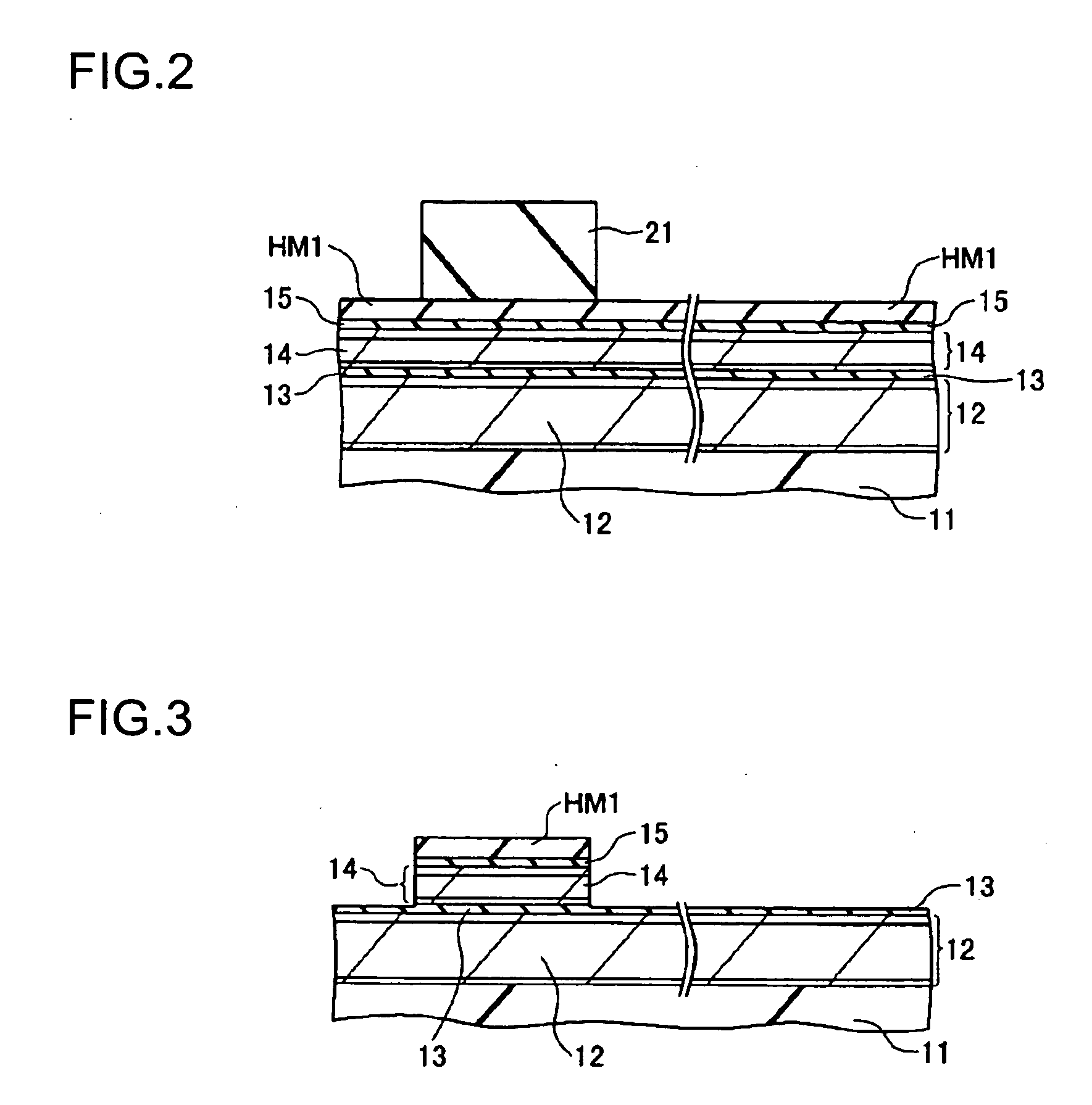
[0021]FIG. 1 is a sectional view showing the structure of an MIM capacitor included in a semiconductor integrated circuit according to a semiconductor device of a first embodiment of the present invention. The integrated circuit having a metal multilayer wiring technology is constructed on a semiconductor substrate. In a part of the integrated circuit, a metal wiring layer 12 is formed on an insulating film 11 in a predetermined layer. The metal wiring layer 12 may be formed of a multilayer of, for example, TiN / Al—Cu alloy / Ti / TiN. The metal wiring layer 12 is patterned together with a hard mask member HM2. In this embodiment the hard mask member HM2 is formed of a SiO-based material and it remains here. The metal wiring layer 12 here forms a plate of a lower capacitor electrode. In other regions, the metal wiring layer 12 forms a usual wiring pattern, a dummy pattern and the like.

[0022] A metal wiring layer 14 is formed on the metal wiring layer 12 with a capacitor insulating film ...


PUM


Abstract

A semiconductor device including an MIM capacitor is provided. A first metal wiring layer is patterned together with a first hard mask member and forms a lower capacitor electrode. A second metal wiring layer is formed on the first metal wiring layer with a capacitor insulating film therebetween and is patterned together with a protection layer and a second hard mask member which remains under the first hard mask member. The second metal wiring layer forms a plurality of upper capacitor electrodes. A third metal wiring layer connected with the first or second metal wiring layer is patterned on an insulating film. The third metal wiring layer includes a connection with a plug wiring member provided within a first or second contact hole.

Description

RELATED APPLICATIONS [0001] This application claims priority to Japanese Patent Application No. 2003-176053 filed Jun. 20, 2003 which is hereby expressly incorporated by reference herein in its entirety. BACKGROUND [0002] 1. Field of the Invention [0003] The present invention relates to a method of manufacturing a semiconductor device and a semiconductor device, and more particularly, the invention relates to a semiconductor device including a capacitor having a metal-insulator-metal (MIM) structure in a metal multilayer wiring which forms an integrated circuit and a method of manufacturing such a semiconductor device. [0004] 2. Description of the Related Art [0005] An MIM capacitor to which a metal multilayer wiring technology is applied has lower parasitic resistance and parasitic capacitance compared to capacitors which have a metal-oxide semiconductor (MOS) structure or electrodes made of polysilicon. Therefore, using such an MIM capacitor may improve the performance of devices....

Claims


Application Information

Patent Timeline
IPC IPC(8): H01L21/02H01L23/52H01L21/033H01L21/3205H01L21/3213H01L21/768H01L21/822H01L21/8242H01L27/04
CPCH01L21/0332H01L28/75H01L21/32139
Inventor YUSA, YOSHINOBU
Owner SEIKO EPSON CORP
Why Eureka
Try Eureka