Method and apparatus for removing an edge region of a layer applied to a substrate and for coating a substrate and a substrate

a technology of edge region and layer, applied in the field of method and apparatus for removing edge region of layer applied to substrate and coating substrate, can solve the problems of unfavorable functional properties, unfavorable photoresist removal, contamination of photoresist layer, etc., and achieve the effect of reliable removal, simple and reliable removal

a technology of edge region and layer, applied in the field of method and apparatus for removing edge region of layer applied to substrate and coating substrate, can solve the problems of unfavorable functional properties, unfavorable photoresist removal, contamination of photoresist layer, etc., and achieve the effect of reliable removal, simple and reliable removal

US20050020087A1Inactive Publication Date: 2005-01-27SCHOTT AG

Image

  • Method and apparatus for removing an edge region of a layer applied to a substrate and for coating a substrate and a substrate
  • Method and apparatus for removing an edge region of a layer applied to a substrate and for coating a substrate and a substrate
  • Method and apparatus for removing an edge region of a layer applied to a substrate and for coating a substrate and a substrate

Examples


first embodiment

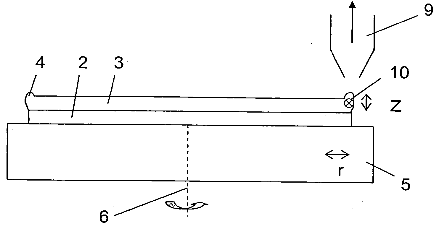
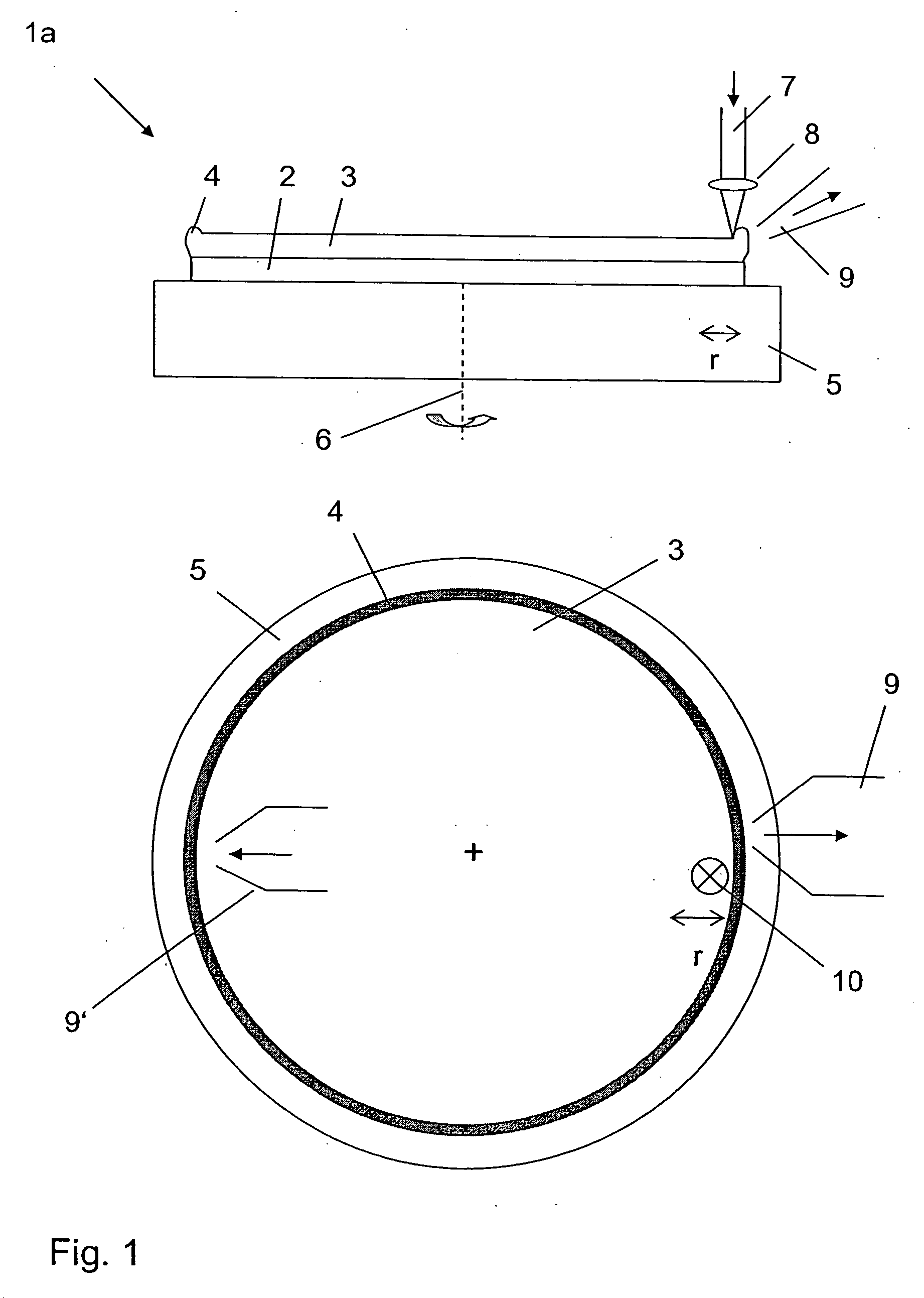
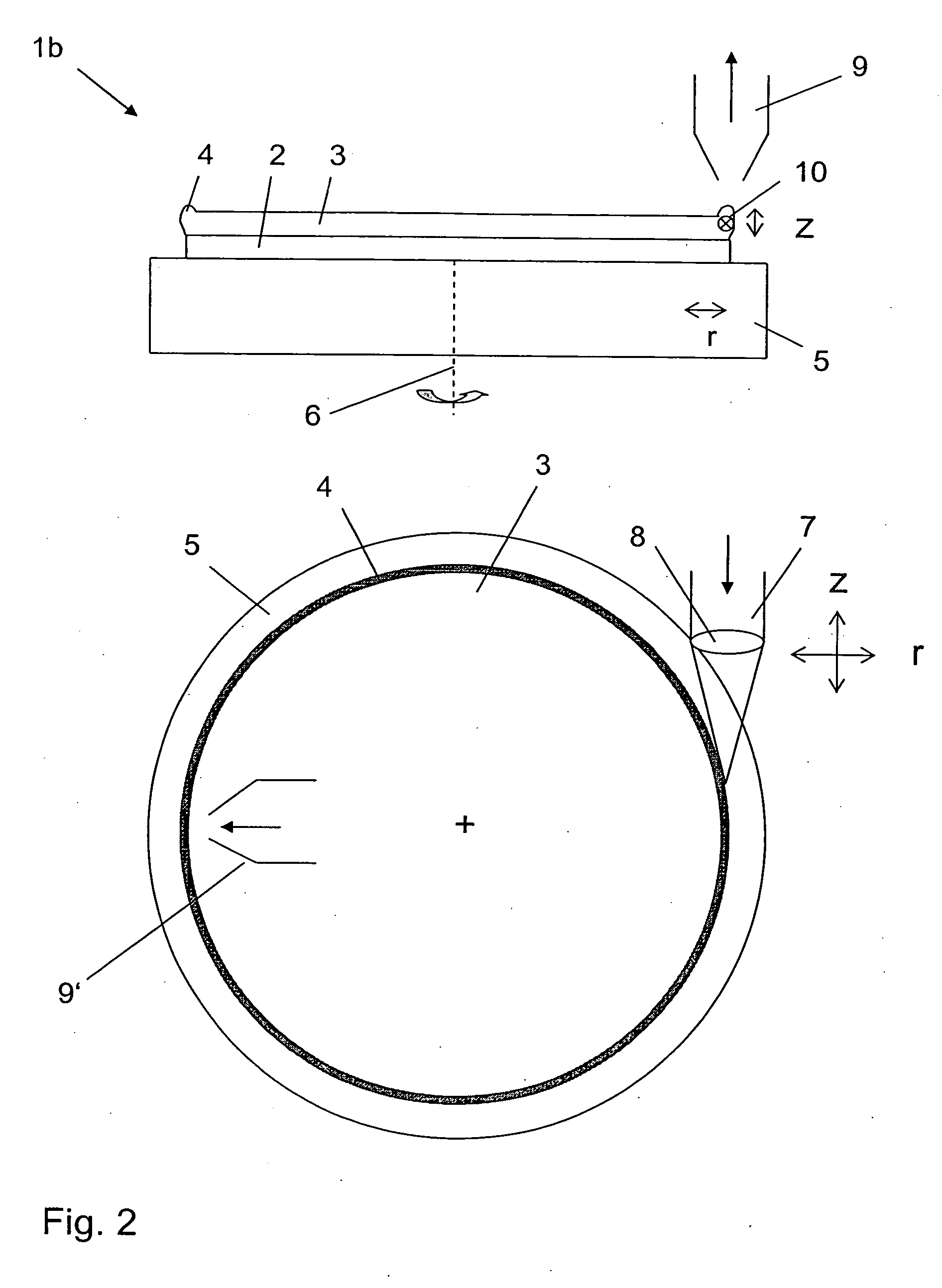
[0039]FIG. 1 shows a schematic cross-section and plan view of an apparatus (hereinafter) 1a according to the present invention. The device 1a comprises a holding means 5, on which a substrate 2 is held. The holding means 5 may, for example, be a vacuum device (vacuum chuck). As indicated by the arrow, the holding means can be rotated about an axis of rotation 6. The holding means 5 may be designed for spin coating a photoresist layer onto the substrate 2, that is to say, for relatively fast rotational velocities. The holding means 5 can also be designed as a holding element in a robot arm or in a production line for semiconductor manufacture.

[0040] A layer 3 is applied to the substrate 2. The edge region 4 of the layer 3 is thickened, as shown schematically in FIG. 1. The term “edge region”, as used in this patent application, always refers to regions of the substrate surface and / or the front face of the circumferential edge of the substrate 2 and / or on the rear side of the substrat...

fourth embodiment

[0050]FIG. 4 shows a schematic perspective view of a device 1d according to the present invention. The device 1d comprises an aperture 12, which is not transparent to the laser beam 7 and which therefore prevents the laser beam 7 from being imaged onto regions of the substrate 2 other than the edge region 4 which is to be removed. The aperture 12 is expediently arranged at a slight distance from the surface of the substrate. Accordingly, diffraction effects can occur close to the edge of the screen 12, thereby providing an additional degree of freedom for specifying and removing an appropriate volume of the edge region 4.

[0051]FIG. 5a shows the results of a mechanical profile measurement of an edge region of a mask blank, which has been removed according to the present invention. A mask blank made from quartz glass was coated with an insoluble and / or hardly soluble electron-beam resist (type ZEP 7000, manufactured by Nippon Zeon) and hardened at a temperature (baking temperature) of...


PUM

PropertyMeasurementUnit
Solubility (mass)aaaaaaaaaa

Abstract

The invention relates to a method and an apparatus for removing an edge region of a layer applied to a substrate and for coating a substrate, in particular, with a photoresist layer. Furthermore, the present invention relates to a substrate, onto which a layer, in particular, a photoresist layer for use in a microlithographic process, is applied, wherein an edge region of the layer is removed according to the invention. In the method, a laser beam is imaged onto the edge region, and the edge region is removed by the laser beam. In this manner, the edge region can be removed reliably and precisely, without damage to or contamination of regions of the layer which are not to be removed.

Description

[0001] Method and apparatus for removing an edge region of a layer applied to a substrate and for coating a substrate and a substrate The present application claims convention priority of German patent application No. 103 18 681.6 the whole contents of which is hereby explicitly incorporated by reference. FIELD OF INVENTION [0002] The present invention relates to a method and an apparatus for removing an edge region of a layer applied to a substrate and for coating a substrate, in particular with a photoresist layer. Furthermore, the present invention relates to a substrate onto which a layer is applied, of which an edge region is removed according to the invention, in particular, a photoresist layer for use in a microlithographic process. BACKGROUND OF THE INVENTION [0003] In the coating of substrates, for example, wafers, maskblanks, photo masks or substrates for use in LCD displays, the peripheral regions and the edges of the substrate are also coated. However, a coating is undes...

Claims


Application Information

Patent Timeline
27 Jan 2005
Publication
US20050020087A1
IPC
B23K26/40; G03F7/20; H01L21/027
CPC
B23K26/0656; B23K26/0738; B23K26/0807; B23K26/0823; G03F7/2028; B23K26/362; B23K26/4075; B23K26/409
Inventors
WAGNER, HERMANN; BEIER, BERND