Manufacturing method of silicon thin film solar cell

a technology of crystalline silicon and solar cells, which is applied in the direction of sustainable manufacturing/processing, final product manufacturing, coatings, etc., can solve the problems of uneven thickness and crystallinity of crystalline thin films formed on the substrate, and achieve the effect of reducing the performance of thin film solar cells

Inactive Publication Date: 2005-02-03
SHARP KK
View PDF8 Cites 105 Cited by
  • Summary
  • Abstract
  • Description
  • Claims
  • Application Information

AI Technical Summary

Benefits of technology

[0009] When a microcrystalline or polycrystalline thin film is used as an i layer of a silicon thin film solar cell, an amount of light absorption at long wavelengths increases and an output current increases as compared with an amorphous thin film. High frequency power to an amount of material gas flow must be increased to form a crystalline thin film with a plasma CVD method as compared with an amorphous thin film. When the high frequency power to the amount of material gas flow is increased, however, material gas is decomposed before uniformly diffuse

Problems solved by technology

Therefore, though a uniform formation of a crystalline thin film on a substrate of a large area is desired, supply and decomposition states of

Method used


Image

  • Manufacturing method of silicon thin film solar cell
  • Manufacturing method of silicon thin film solar cell
  • Manufacturing method of silicon thin film solar cell

Examples


first example

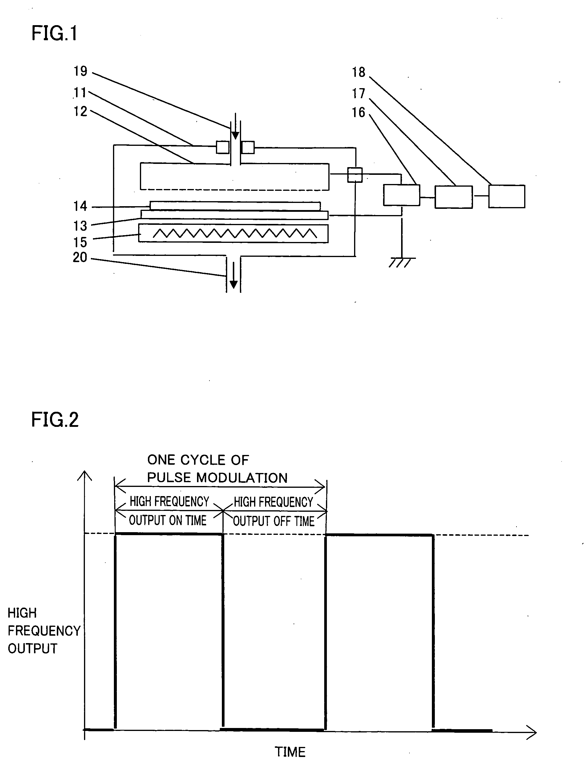
[0045] Three chambers as reaction chamber 11 of the manufacturing apparatus shown in FIG. 1 were prepared and connected in a line via gate valves. A silicon thin film solar cell was manufactured with the manufacturing method according to the present invention using an apparatus wherein p, i and n layers of the silicon thin film can be formed on a substrate respectively in the three reaction chambers with the high frequency plasma CVD method.

[0046] A glass substrate of a large area having a size of 1000 mm×500 mm and having a transparent conductive layer formed on a surface thereof was used as the substrate. The substrate was heated to about 200° C. in a first reaction chamber, and then mixed gas of SiH4, H2 and B2H6 was introduced as material gas, and high frequency power of continuous wave was applied to the electrode to form a p type microcrystalline silicon layer on the substrate. Then the substrate was moved to a second reaction chamber, whereinto mixed gas of SiH4 and H2 was i...

second example

[0054] Six chambers as reaction chamber 11 of the manufacturing apparatus shown in FIG. 1 were prepared and connected in a line via gate valves. A silicon thin film solar cell was manufactured with the manufacturing method according to the present invention using an apparatus wherein p, i, n, p, i, and n layers of the silicon thin film can be formed on a substrate respectively in the six reaction chambers with the high frequency plasma CVD method.

[0055] A glass substrate of a large area having a size of 1000 mm×1000 mm and having a transparent conductive layer formed on a surface thereof was used as the substrate. The substrate was heated to about 200° C. in a first reaction chamber, and then mixed gas of SiH4, H2, CH4, and B2H6 was introduced as material gas, and high frequency power of continuous wave was applied to the electrode to form a p type amorphous silicon carbide layer on the substrate. Then the substrate was moved to a second reaction chamber, whereinto mixed gas of SiH...


PUM

PropertyMeasurementUnit
Timeaaaaaaaaaa
Timeaaaaaaaaaa
Areaaaaaaaaaaa

Abstract

To uniformly form a silicon thin film for a solar cell, having an i layer formed with crystalline silicon, on a substrate of a large area to provide a high power solar cell, in a manufacturing method of a silicon thin film solar cell, a silicon thin film, having a structure such that an i layer is sandwiched between a p layer and an n layer, is formed on a substrate with a high frequency plasma CVD method, wherein i layer is formed with crystalline silicon using plasma with pulse-modulated high frequency power, one cycle of pulse modulation includes an ON state for outputting high frequency power and an OFF state for not outputting, an output waveform is modulated to be rectangular, a time of the ON state is 1-100 microseconds, and a time of the OFF state is 5 microseconds or longer.

Description

[0001] This nonprovisional application is based on Japanese Patent Application No. 2003-203707 filed with the Japan Patent Office on Jul. 30, 2003 the entire contents of which are hereby incorporated by reference. BACKGROUND OF THE INVENTION [0002] 1. Field of the Invention [0003] The present invention relates to a method of forming a crystalline silicon thin film in a silicon thin film solar cell. [0004] 2. Description of the Background Art [0005] A kind of general silicon thin film solar cell has a structure such that, on a translucent insulation substrate of glass or the like, a transparent conductive film of SnO2, ITO or the like is formed, and then a p layer, an i layer and an n layer, or an n layer, an i layer and a p layer of amorphous semiconductor are respectively stacked thereon in this order to form a photoelectric conversion active layer, on which a backside electrode of a metal thin film is stacked. Another kind has a structure such that, an n layer, an i layer and a p ...

Claims


Application Information

Patent Timeline
IPC IPC(8): C23C16/24C23C16/515H01L31/04H01L31/075H01L31/076H01L31/077H01L31/18
CPCC23C16/24C23C16/515Y02E10/548H01L31/1824Y02E10/545H01L31/076Y02E10/547Y02P70/50
Inventor FUJIOKA, YASUSHISHIMIZU, AKIRAFUKUDA, HIROYUKINOMOTO, KATSUHIKO
Owner SHARP KK
Why Eureka
Try Eureka