
Providing a register file memory with local addressing in a SIMD parallel processor

Inactive Publication Date: 2005-02-03
MICRON TECH INC
View PDF24 Cites 28 Cited by
  • Summary
  • Abstract
  • Description
  • Claims
  • Application Information

AI Technical Summary

Benefits of technology

[0009] In accordance with this invention a register file memory with partial local addressing is provided that minimizes the increase in hardware complexity and cost. A single instruction multiple data (SIMD) array (e.g., a processing element array) can be integrated with a main memory, typically dynamic random access memory (DRAM), on a single chip. A simple SIMD array can be divided into the following: a register file memory, one or more processing elements, a control logic sequencer, an interconnect, and a memory buffer register. The register file memory is preferably implemented using static random access memory (SRAM) because SRAM is more area efficient for large memories compared to other types of memory. Two major area overheads for the register file SRAM are (1) decode logic and (2) read logic and sense amplifiers (RLSAs). Decode logic decodes an address in the register file SRAM. RLSAs provide a method of reading data from or writing data to the decoded address. Each processing element processes data from its own block of the register file SRAM. The control logic sequencer can direct the processing of data in each processing element and control data flow between processing elements via the interconnect. The control logic sequencer can also direct the transfer of data between each processing element and a partitioned block of DRAM via memory buffer registers. Data may flow from each block of DRAM to the SIMD array via data paths.
[0010] To minimize the hardware complexity and cost associated with full local addressing, partial local addressing is implemented for the register file SRAM. Instead of allocating a unique register file SRAM (e.g., an 8-bit wide SRAM) for each processing element, multiple processing elements (e.g., 8) can be assigned to a register file SRAM (e.g., a 64-bit wide SRAM). Because the decode logic and RLSAs are roughly constant in size in one-dimension regardless of the depth and width of the register file SRAM, this generally results in less area overhead for the 64-bit wide SRAM compared to its equivalent of eight 8-bit wide SRAMs.
[0020] The SIMD array and memory is typically integrated onto a single chip using a layout design. Because of the need to pitch match (a method of layout that minimizes the routing of wire connections between components) the SIMD array to the DRAM, the layout of the system typically contains extra space between the bytes. Thus, the additional bits cells and logic may be added within the extra spaces, resulting in little or no area overhead.

Problems solved by technology

There are penalties associated with this form of local autonomy.
Another penalty for implementing local addressing is the additional hardware needed for each processing element to generate and deliver an address to its own block of memory.
The area and cost overhead is typically very high and thus many SIMD parallel processors do not implement local addressing.

Method used


Image

  • Providing a register file memory with local addressing in a SIMD parallel processor
  • Providing a register file memory with local addressing in a SIMD parallel processor
  • Providing a register file memory with local addressing in a SIMD parallel processor

Examples


Embodiment Construction

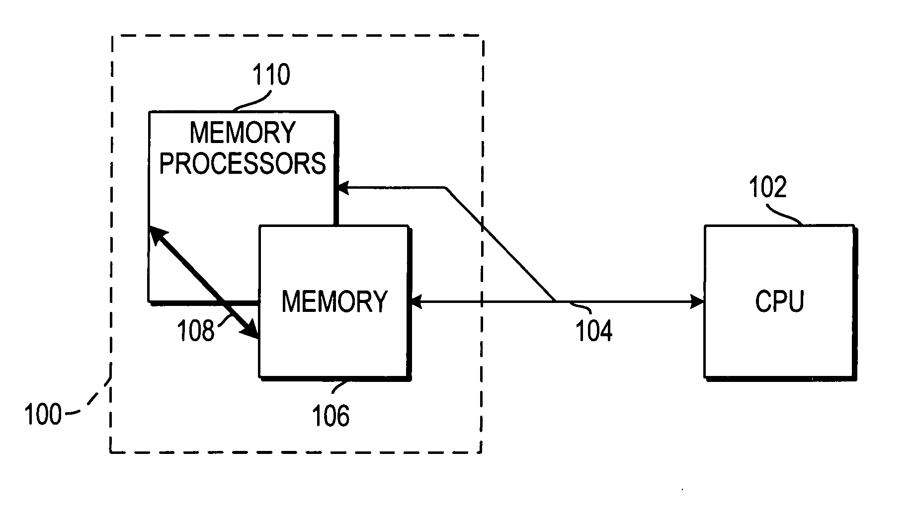
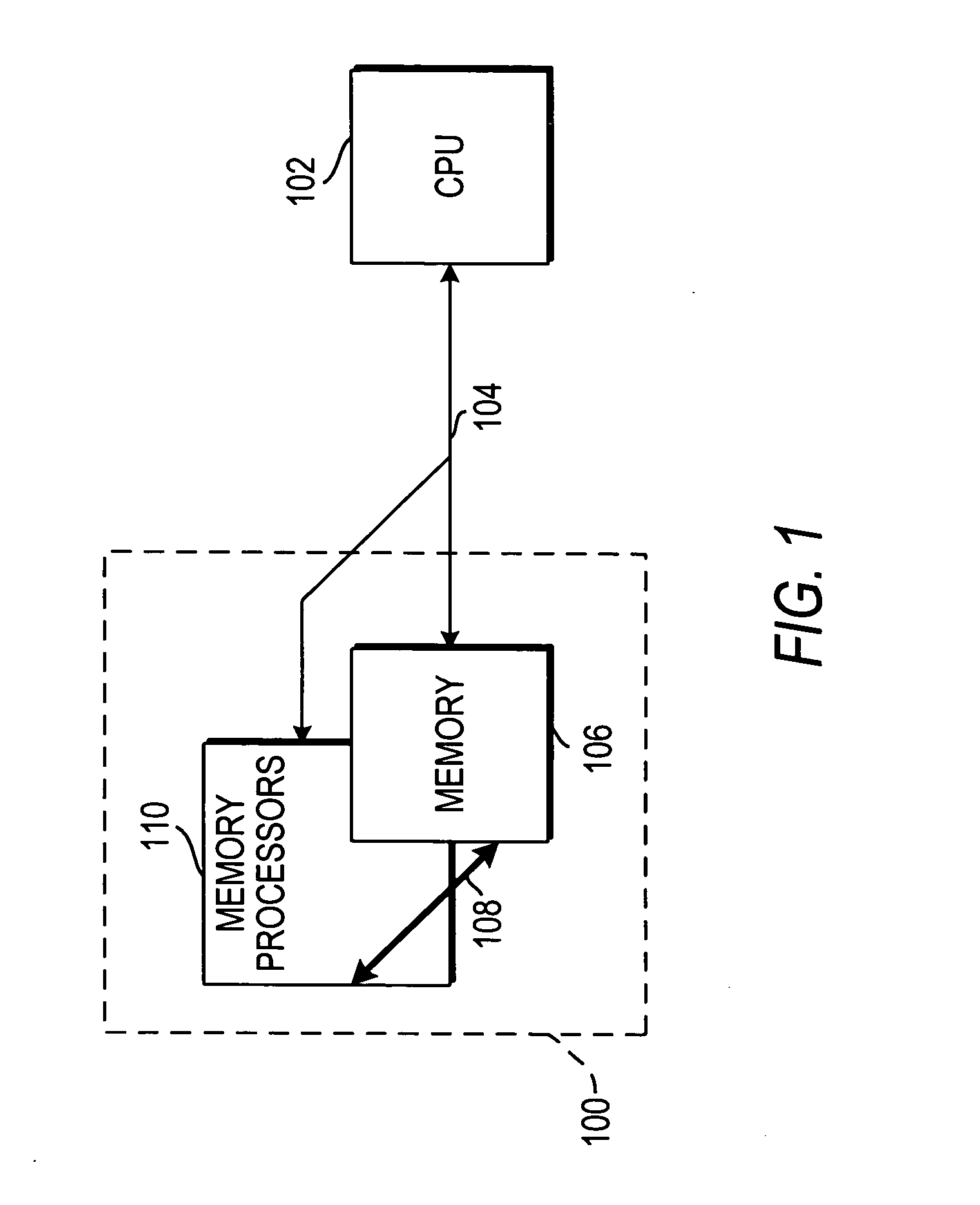
[0037]FIG. 1 illustrates one embodiment of an active memory block in accordance with the invention. Active memory block 100 can include a memory 106 and memory processors 110. Memory 106 is preferably random access memory (RAM), in particular dynamic RAM (DRAM). Memory processors 110, which include processing element (PE) arrays, can communicate with memory 106 via an interconnection block 108. Interconnection block 108 can be any suitable communications path, such as a bi-directional high memory bandwidth path. A central processing unit (CPU) 102 can communicate with active memory block 100 via a communications path 104. Communications path 104 may be any suitable bi-directional path capable of transmitting data.

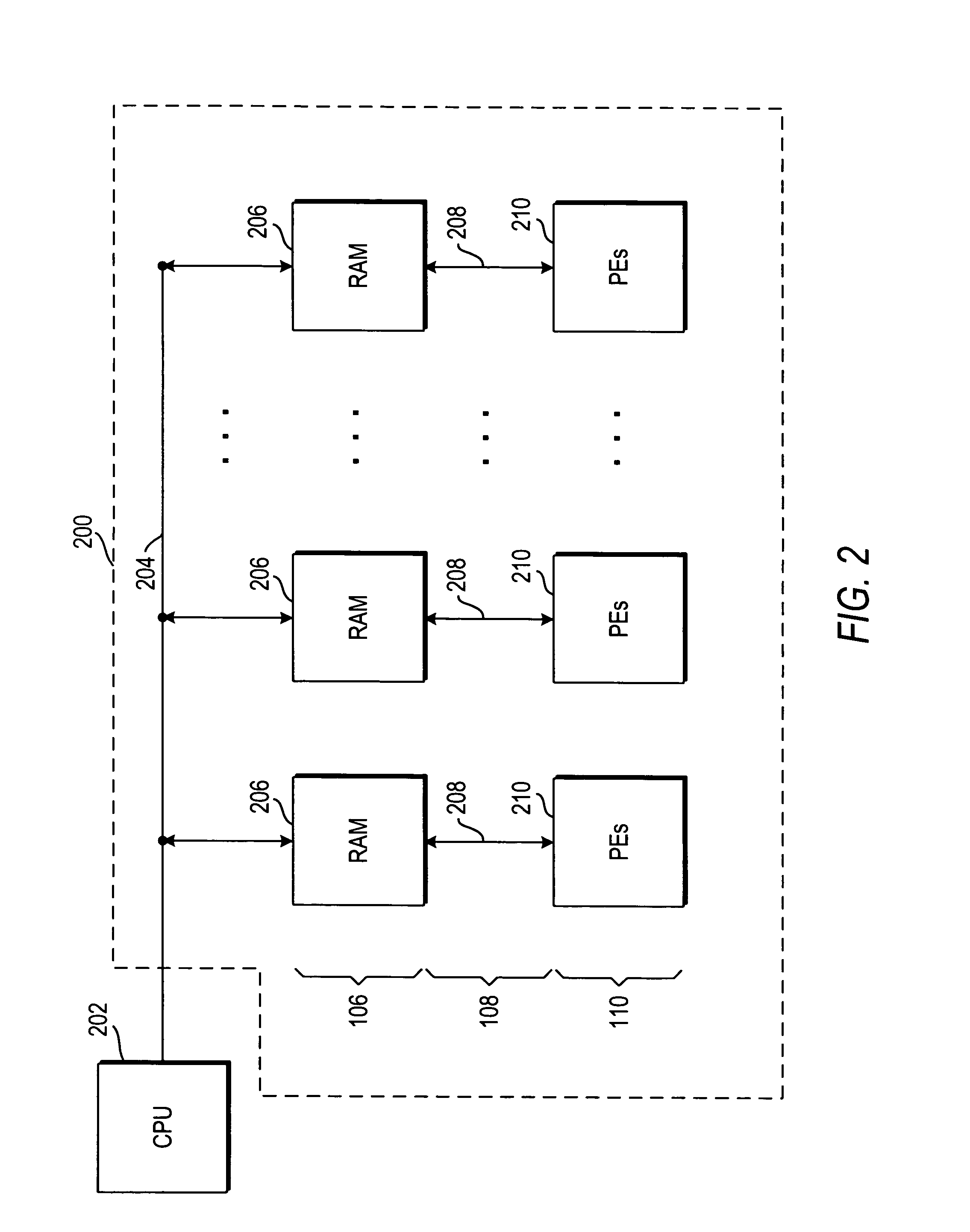
[0038]FIG. 2 illustrates one embodiment of a partitioned active memory block 200 in accordance with the invention. A unique range of memory addresses may be allocated to each processing element array 210, thereby allowing each processing element array 210 to operate on its...


PUM


Abstract

A degree of local addressing is provided for a processing element array by partitioning a register file memory (e.g., data columns, data rows), and adding a select column or row to be associated with each block. The select column or row allows each processing element to read data from or to write data to a different register file address. Global addressing may also be implemented by reading data from or writing data to the same register file address for each processing element. The invention provides the advantage of faster overall execution time, In addition, there is minimal additional area overhead because of the need to pitch match the processing element array to a main memory.

Description

BACKGROUND OF THE INVENTION [0001] This invention relates to local addressing for a register file memory. More particularly, this invention relates to local addressing for a register file memory in a single instruction multiple data (SIMD) parallel processor. [0002] A basic computer generally includes a central processing unit (CPU) and a main memory. The CPU implements a sequence of operations encoded in a stored program. The program and data on which the CPU acts is typically stored in the main memory. The processing of the program and the allocation of main memory and other resources are controlled by an operating system. In operating systems where multiple applications may share and partition resources, the computer's processing performance can be improved by partitioning main memory and developing active memory. [0003] Active memory is memory that processes data as well as stores data. It can be told to operate on its contents without transferring those contents to the CPU or t...

Claims


Application Information

Patent Timeline
IPC IPC(8): G06F9/30G06F15/80
CPCG06F9/30141G06F9/345G06F9/3879G06F15/7821G06F15/8007G06F15/8023G06F9/3885G06F12/0207G06F12/06G06F12/0692G06F15/80G11C8/00G11C8/04G11C8/12
Inventor KIRSCH, GRAHAM
Owner MICRON TECH INC
Learn More