Method of making the selection gate in a split-gate flash EEPROM cell its and structure

a split-gate flash eeprom and selection gate technology, which is applied in the direction of semiconductor devices, electrical apparatus, transistors, etc., can solve the problems of poor writing efficiency and difficulty in making sub-micron-scale split-gate flash eeproms, so as to improve data writing efficiency, reduce the sidewise dimension of the selection gate, and improve the effect of data writing efficiency

Inactive Publication Date: 2005-02-03
TAIWAN SEMICON MFG CO LTD
View PDF9 Cites 3 Cited by
  • Summary
  • Abstract
  • Description
  • Claims
  • Application Information

AI Technical Summary

Benefits of technology

[0012] Not only can the disclosed split-gate flash EEPROM structure effectively reduce the sidewise dimension of the selection gate while maintaining an appropriate channel length, hot ballistic electrons are produced to go along the selection gate channel on the sidewall of the semiconductor substrate trench to the suspending gate. This can improve the data writing efficiency and lower the writing voltage. Therefore, the invention achieves the goal of a high access speed and low power consumption for the split-gate flash EEPROM manufactured in a deep submicron process.

Problems solved by technology

If the channel length is too short, short channel effects may happen; while if the channel length is too long, the writing efficiency will be bad.
Therefore, there is some difficulty in making submicron-scale split-gate flash EEPROM.

Method used


Image

  • Method of making the selection gate in a split-gate flash EEPROM cell its and structure
  • Method of making the selection gate in a split-gate flash EEPROM cell its and structure
  • Method of making the selection gate in a split-gate flash EEPROM cell its and structure

Examples


Embodiment Construction

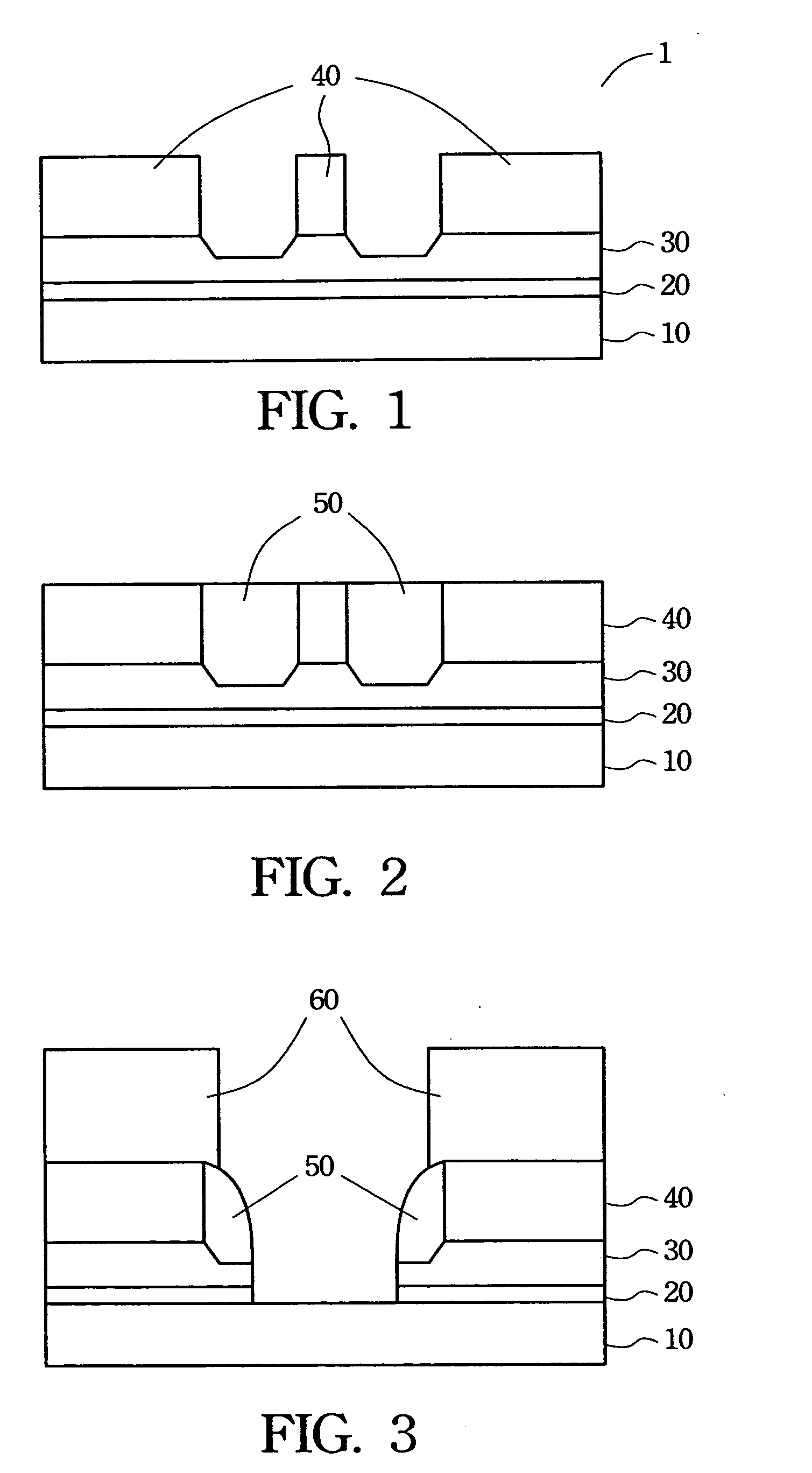
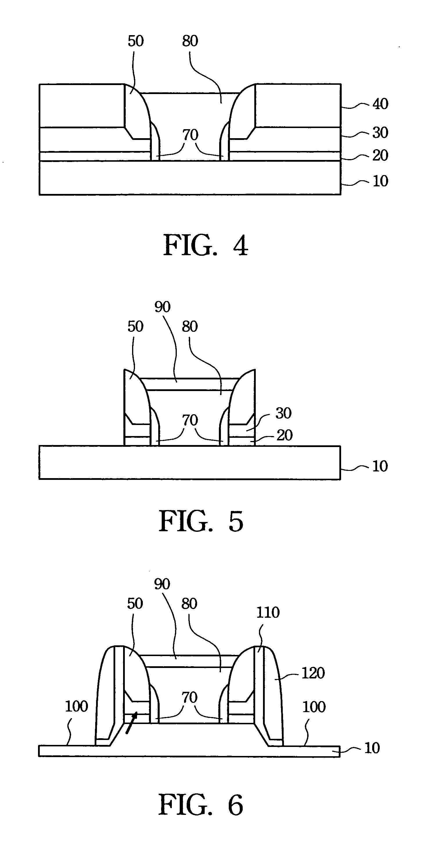
[0016] The invention discloses a split-gate flash EEPROM cell structure and the associated manufacturing method. The selection gate of the split-gate flash EEPROM is formed on the sidewall of a semiconductor substrate trench, using the trench sidewall as the selection gate channel. The invention can maintain an appropriate channel length while minimizing the sidewise dimension of the selection gate. Such a channel structure can produce ballistic hot electrons to improve the data writing efficiency and to lower the writing voltage.

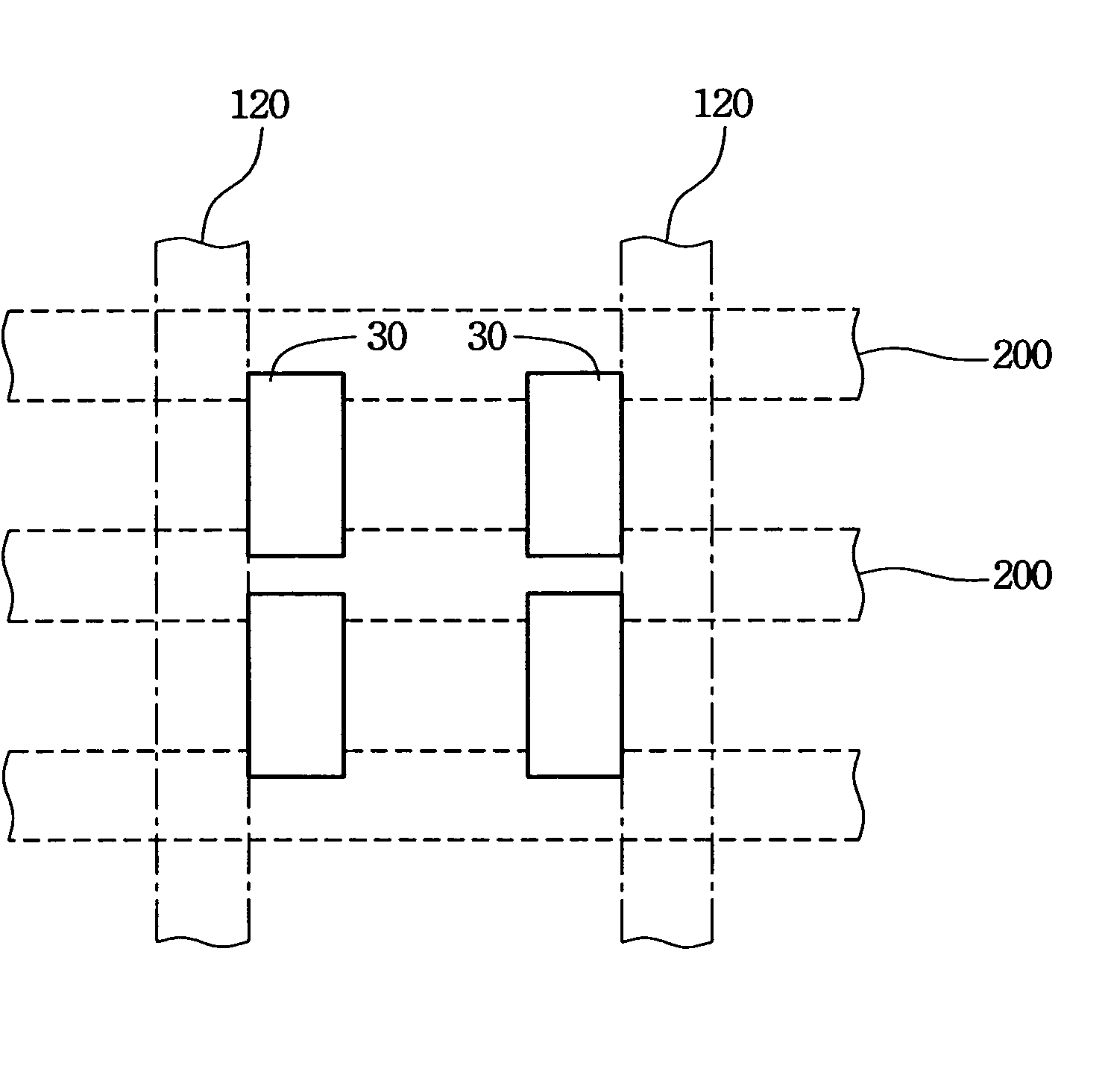
[0017]FIG. 1 shows the initial structure for making the disclosed split-gate flash EEPROM cell. As shown in the drawing, the memory cell 1 contains a semiconductor substrate 10, a gate oxide layer 20, a polysilicon layer 30, and a silicon nitride layer 40. Preferably, the substrate 10 can be a single crystal semiconductor material with the crystalline direction. The gate oxide layer 20 is an oxide layer with thickness between 50 Å and 150 Å is formed on t...


PUM


Abstract

A method of making the selection gate in a split-gate flash EEPROM cell forms a selection gate on a trench sidewall of a semiconductor substrate to minimize the sidewise dimension of the selection gate and to maintain the channel length. The disclosed method includes the steps of: forming a trench on a semiconductor substrate on one side of a suspending gate structure; forming an inter polysilicon dielectric layer on the sidewall of the suspending gate structure and the trench; and forming a polysilicon spacer on the inter polysilicon dielectric layer as the selection gate. Such a split-gate flash EEPROM cell can produce ballistic hot electrons, improving the data writing efficiency and lowering the writing voltage.

Description

BACKGROUND OF THE INVENTION [0001] 1. Field of Invention [0002] The invention relates to a semiconductor device and the associated manufacturing process. In particular, it relates to a manufacturing method of the selection gate in a split-gate flash EEPROM cell. [0003] 2. Related Art [0004] Typically, the data storage media in computers can be separated into volatile and nonvolatile memory. The volatile memory includes the dynamic random access memory (DRAM) and static random access memory (SDRAM). Since the data stored in such memory will disappear immediately after the power supply is interrupted, it is mainly used in temporary data input / output (I / O). The nonvolatile memory can keep the stored data even after the power supply is turned off. Therefore, such memory can be used in various occasions. The nonvolatile memory can be divided according to the access method into mask read only memory (ROM), erasable programmable read only memory (EPROM), electric erasable programmable read...

Claims


Application Information

Patent Timeline
Patent Type & Authority Applications(United States)
IPC IPC(8): H01L21/28H01L21/336H01L21/8247H01L27/115H01L29/423H01L29/788
CPCH01L21/28273H01L27/115H01L29/7885H01L29/42324H01L29/66553H01L27/11521H01L29/40114H10B69/00H10B41/30
Inventor CHU, WEN-TINGYEH, JACKLIN, CHRONG-JUNG
Owner TAIWAN SEMICON MFG CO LTD
Why Eureka
Try Eureka