Plasma etching using dibromomethane addition

a dibromomethane addition and etching technology, applied in the field of anisotropic plasma etching of silicon, can solve the problems of inability to achieve reasonable reliability, low etching efficiency, and low etching efficiency, and achieve the effect of inhibiting the formation of compounds

Inactive Publication Date: 2005-02-10
MICROSEMI CORP POWER PRODS GROUP
View PDF8 Cites 5 Cited by
  • Summary
  • Abstract
  • Description
  • Claims
  • Application Information

AI Technical Summary

Benefits of technology

[0014] In one aspect of the present invention, there is provided a plasma etch chemistry which has been shown to be capable of nearly perfectly vertical etching of silicon or materials having a significant silicon content, yet it does not present the problems noted above by the prior art. In a preferred embodiment, dibromomethane is added thereto, and anisotropic etching is provided. This is accomplished by the adsorption of a Si—Br compound on the sidewalls of the etch cavity, while the ion bombardment on the flat surface inhibits the formation of the compound in that area. The silicon may be etched as Si—Cl—Br compound.
[0015] Dibromomethane is a relatively safe gas and not ozone depleting, yet giving substantially similar results in plasma etching of silicon, silicon nitride, and other materials, and therefore is an improvement over the prior art.

Problems solved by technology

The fragile nature of the small geometry structures cannot have a reasonable degree of reliability if any significant amount of undercutting takes place during the process.
However, some silicon materials, such as highly doped polysilicon, still experience some undercutting if etch conditions are not closely controlled.
Furthermore, the use of chlorocarbons as the Cl source for etching polysilicon is not desirable.
Selectivity to the underlying SiO2 layer is a constant problem because the C is a good reducer of SiO2, combining with the O to form CO and CO2.

Method used


Image

  • Plasma etching using dibromomethane addition
  • Plasma etching using dibromomethane addition

Examples


Embodiment Construction

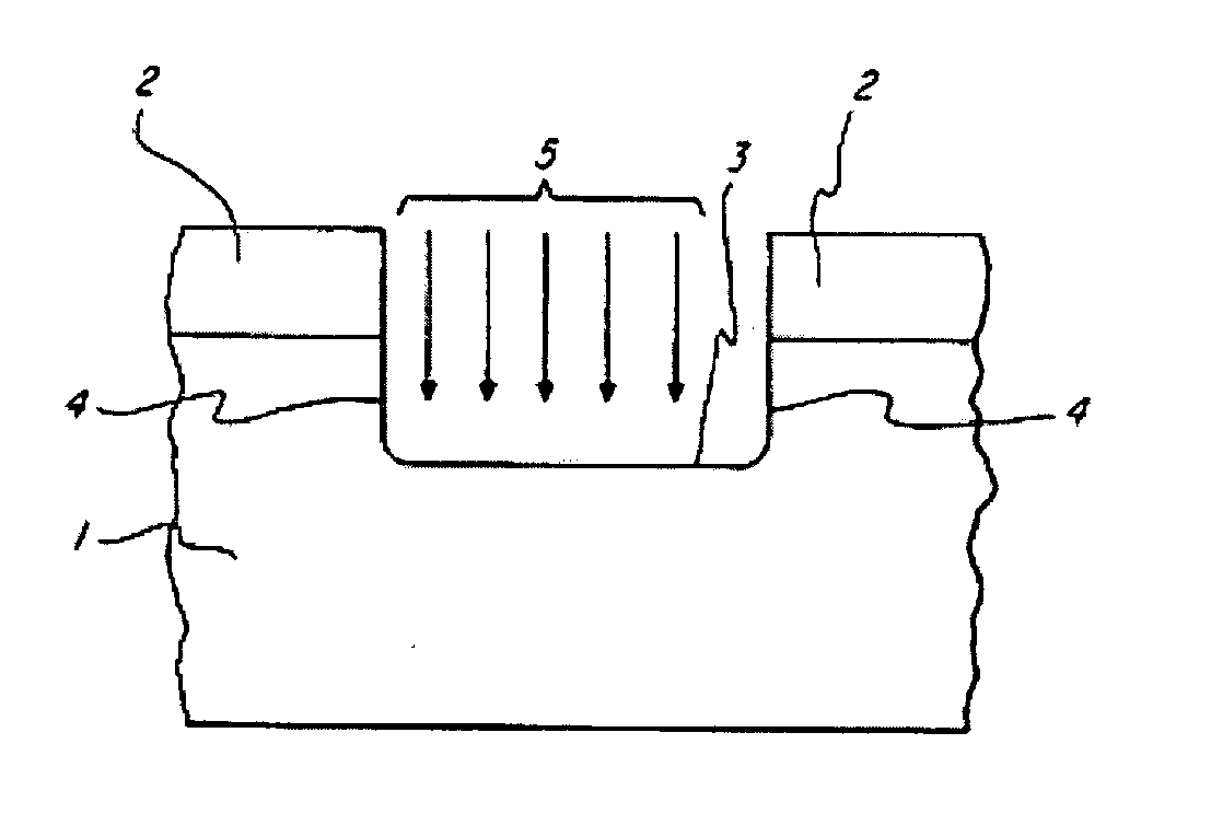
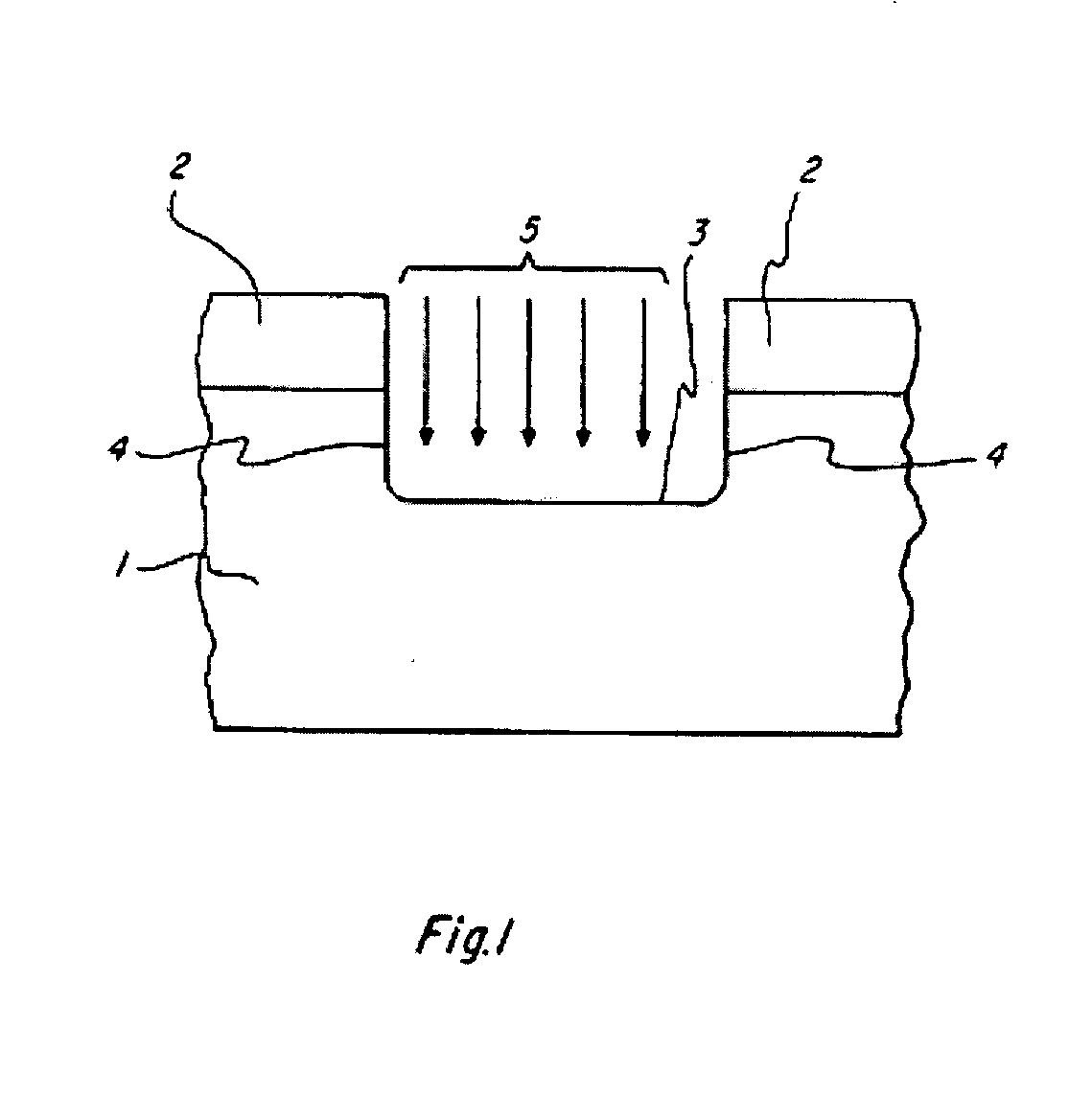
[0018] The present invention teaches that a highly anisotropic etch can be achieved by the addition of dibromomethane to the silicon etching chemistry. Ion bombardment overcomes the resistance to etching on flat surfaces, but lateral etching can be suppressed by the formation of a Si—Br compound on the sidwalls.

[0019] A five (5) wafer Reactive Ion Etch plasma reactor was used for the following experiments. The wafers rested on the unpowered 12 inch diameter quartz plate which in turn rested on an anodized aluminum electrode.

[0020] The counter electrode was stainless steel. The RF frequency was 13.56 MHz. The process conditions for the etching of heavily phosphorus doped polysilicon were as follows:

[0021] SiCl4=200 sccm

[0022] Cl2=20 sccm

[0023] Power=200 watts

[0024] Temp.=60.degree. C.

[0025] Plate Spacing=1 inch

[0026] Pressure=20 milliTorr.

[0027] The polysilicon etch rate was about 500 angstroms / min. After 50% overetch, the polysilicon was severely undercut, indicating essent...


PUM


Abstract

The disclosure relates to a plasma etch chemistry which allows a near perfectly anisotropic etch of silicon. A Cl-based plasma etch such as SiCl4+Cl2 has CH2Br2 added thereto, readily allowing the anisotropic etching of silicon. The silicon surface facing the discharge is subjected to ion bombardment, allowing the volatilization (etching) of silicon as a Si—Cl—Br compound. The Br which adsorbs on the sidewalls of the etched silicon passivates them from the etching. This new plasma etch chemistry yields a very smooth etched surface, and the etch rate is relatively insensitive to the electrical conductivity of the silicon. The use of dibromomethane is an improvement over the prior art which typically used HBr; a poisonous and ozone depleting gas. Dibromomethane is a relatively safe gas and not ozone depleting, yet giving substantially similar results in plasma etching of silicon, silicon nitride, and other materials.

Description

CROSS REFERENCE TO RELATED APPLICATIONS [0001] This application claims priority from U.S. Provisional Application No. 60 / 493,686, filed on Aug. 7, 2003, which is incorporated herein by reference.BACKGROUND OF THE INVENTION [0002] 1. Field of the Invention [0003] This invention relates to the field of semiconductor devices and, more particularly, to anisotropic plasma etching of silicon. [0004] 2. Description of the Prior Art [0005] Plasma etch processes currently used to etch materials for semiconductor device fabrication consist of an electrical discharge of halogen bearing gases. Halogens typically encountered in these processes are fluorine, chlorine and bromine. The process begins with application of a masking material, such as photoresist, to protect the desired geometry of the device from the etch process. The device in process is then placed in a plasma reactor and etched. The subsequent steps are determined by the type of device being fabricated. This process is especially v...

Claims


Application Information

Patent Timeline
Patent Type & Authority Applications(United States)
IPC IPC(8): G01R31/00H01LH01L21/3065H01L21/3213
CPCH01L21/32137H01L21/3065
Inventor LEVERICH, LYLE T.
Owner MICROSEMI CORP POWER PRODS GROUP
Why Eureka
Try Eureka