
Custom electrodes for molecular memory and logic devices

a logic device and molecular memory technology, applied in the field of nanoscale computing and memory circuits, can solve the problems of decreasing the number of electrons either accessed or utilized within the device, becoming increasingly difficult to design well-behaved devices, and increasing the difficulty of fabrication and cost, so as to achieve low diffusion, high bulk modulus, and high melting point

Inactive Publication Date: 2005-02-10
BECK PATRICIA A +3
View PDF32 Cites 3 Cited by
  • Summary
  • Abstract
  • Description
  • Claims
  • Application Information

AI Technical Summary

Benefits of technology

This approach results in stable, conductive electrodes with controlled oxide formation, high melting point, and low diffusion, enabling efficient fabrication of molecular electronic devices with improved conductivity and compatibility with various deposition techniques, addressing the limitations of prior materials like gold and polysilicon.

Problems solved by technology

As feature sizes of integrated-circuit devices continue to decrease, it becomes increasingly difficult to design well-behaved devices.
The fabrication is also becoming increasingly difficult and expensive.
In addition, the number of electrons either accessed or utilized within a device is decreasing, which produces increased statistical fluctuations in the electrical properties.
Aluminum forms a poorly controlled native oxide that acts as a natural barrier to electronic transport.
Platinum is difficult to maintain in a stable form.
Working with a just-deposited-film (perhaps the “cleanest” way) is difficult and impractical.
Shadow masks avoid lithographic process, but are dimensionally limited (to large micron-sized dimensions, sparsely placed).
Even nano-imprinting exposes surfaces to organic chemicals that are potentially incompatible with the use of organic active layers.

Method used


Image

  • Custom electrodes for molecular memory and logic devices
  • Custom electrodes for molecular memory and logic devices

Examples


examples

[0090] Experimental Procedure

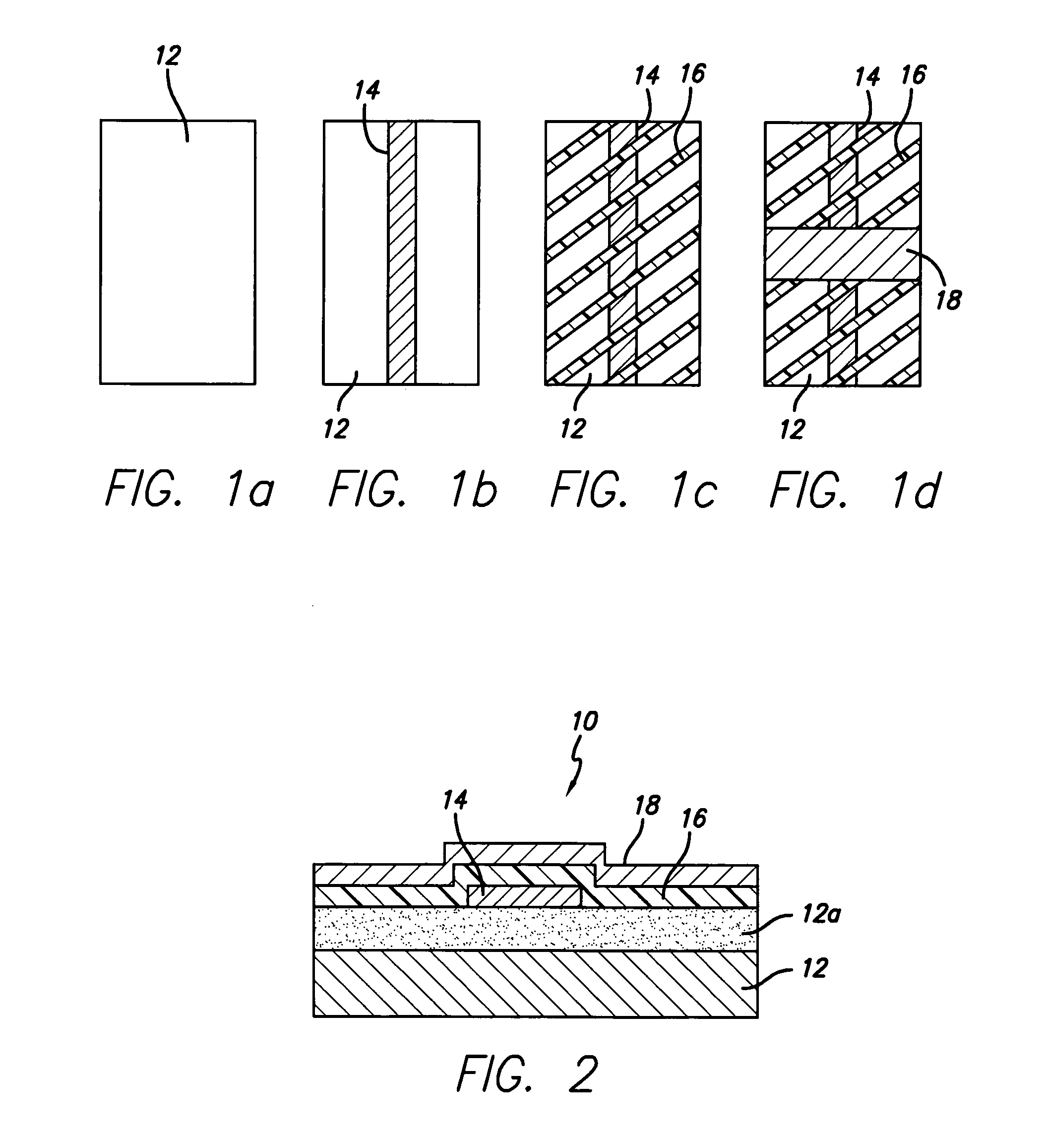
[0091] Both the blanket and photolithographically-modified Pt films were sputter deposited on Si wafers with a 100 nm silicon dioxide layer. The typical Pt thickness was 100 nm. The plasma treatment was performed in a RIE® model 1700 system. Freshly deposited Pt films and films exposed to various plasma treatments were analyzed with contact angle and ellipsometry measurements within 10 minutes of preparation and by XPS and Auger with controls.

[0092] For contact angle measurements a droplet of 2 μL 18 MΩ·cm water was injected onto the sample surface from a syringe. An image of the static water droplet was recorded with a digital camera and analyzed to yield a sessile contact angle, averaging at least three readings.

[0093] Ellipsometric measurements were performed using a laser with a wavelength of 532 nm and an incident angle of 58 degrees. A simple model was used to derive the optical constants, n and k. The platinum was approximated by an infinite th...


PUM

PropertyMeasurementUnit
timeaaaaaaaaaa
timeaaaaaaaaaa
pressureaaaaaaaaaa

Abstract

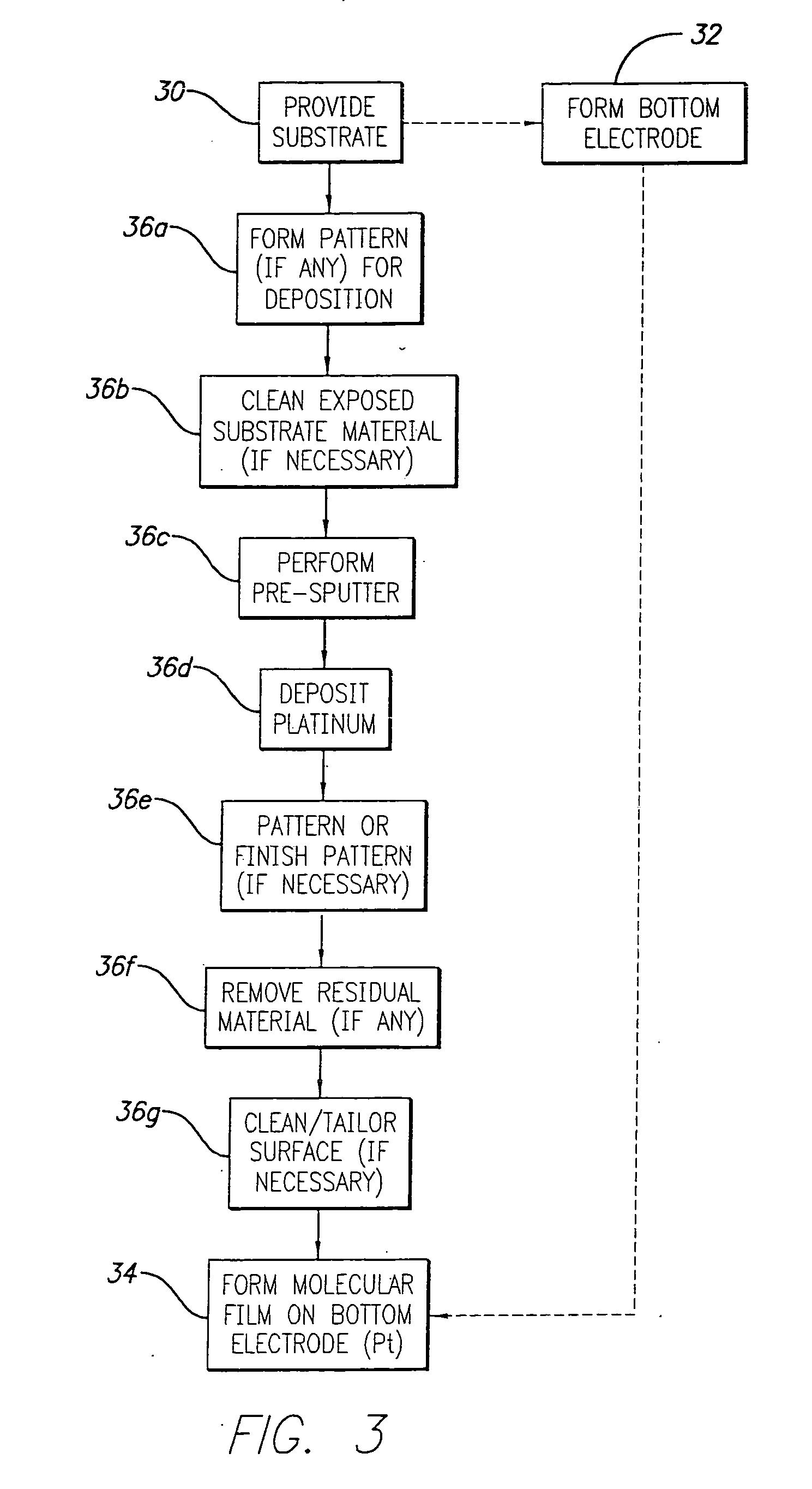
A method is provided for fabricating molecular electronic devices comprising at least a bottom electrode and a molecular switch film on the bottom electrode. The method includes forming the bottom electrode by a process including: cleaning portions of the substrate where the bottom electrode is to be deposited; pre-sputtering the portions; depositing a conductive layer on at least the portions; and cleaning the top surface of the conductive layer. Advantageously, the conductive electrode properties include: low or controlled oxide formation (or possibly passivated), high melting point, high bulk modulus, and low diffusion. Smooth deposited film surfaces are compatible with Langmuir-Blodgett molecular film deposition. Tailored surfaces are further useful for SAM deposition. The metallic nature gives high conductivity connection to molecules. Barrier layers may be added to the device stack, i.e., Al2O3 over the conductive layer.

Description

CROSS-REFERENCE TO RELATED APPLICATIONS [0001] The present application is related to U.S. Pat. No. 6,459,095, issued Oct. 1, 2002, entitled “Chemically Synthesized and Assembled Electronic Devices”, which is directed to the formation of nanowires used for nanoscale computing and memory circuits. The present application is also related to U.S. Pat. No. 6,314,019, issued Nov. 6, 2001, entitled “Molecular Wire Crossbar Interconnect (MWCI) for Signal Routing and Communications”, and to U.S. Pat. No. 6,128,214, entitled “Molecular Wire Crossbar Memory”, issued on Oct. 3, 2000, as well as to applications Ser. No. 09 / 280,045, entitled “Molecular Wire Crossbar Logic (MWCL)”, and Ser. No. 09 / 280,188, entitled “Molecular Wire Transistor (MWT)”, both filed on Mar. 29, 1999, which are all directed to various aspects of memory and logic circuits utilized in nanocomputing. The present application is also related to application Ser. No. 09 / 823,195, filed Mar. 29, 2001, entitled “Bistable Molecular...

Claims


Application Information

Patent Timeline
Patent Type & Authority Applications(United States)
IPC IPC(8): H01L21/28G11C13/02H01L21/285H01L27/28H01L29/06
CPCG11C13/02H01L27/28H01L2924/0002H01L2924/00H10K19/00
Inventor BECK, PATRICIA A.OHLBERG, DOUGLASSTEWART, DUNCANLI, ZHIYONG
Owner BECK PATRICIA A
Learn More