Magneto-resistive effect element and magnetic memory

a magnetic memory and effect element technology, applied in the direction of spin-exchange-coupled multilayers, instruments, substrates/intermediate layers, etc., can solve the problems of inability to keep heat stability of magnetic materials, extremely poor thermal stability of bits of the plurality of magnetic domains, and inability to make a memory cell smaller than the size of a semiconductor dram (dynamic random access memory), etc., to achieve excellent heat stability and keep stable magnetic domains.

Inactive Publication Date: 2005-02-24
KK TOSHIBA
View PDF4 Cites 41 Cited by
  • Summary
  • Abstract
  • Description
  • Claims
  • Application Information

AI Technical Summary

Benefits of technology

[0025] The present invention has been made on the basis of recognition of the above problems, and has as its object to provide a magneto-resistive effect element that has excellent heat stability even though the element is miniaturized and that can keep stable magnetic domains even though switching is repeated any number of times, and a magnetic memory having the magneto-resistive effect element in a memory cell.
[0026] A magneto-resistive effect element according to a first aspect of the present invention includes: a magnetization-pinned layer including a magnetic film having a spin moment oriented in a direction perpendicular to a film surface thereof and pinned in the direction; a magnetic recording layer having a spin moment oriented in a direction perpendicular to a film surface thereof; a nonmagnetic layer formed between the magnetization-pinned layer and the magnetic recording layer; and an anti-ferromagnetic film formed on at least side surfaces of the magnetization-pinned layer.
[0027] A magnetic memory according to a second aspect of the present invention includes at least a memory cell, the memory cell including a magneto-resistive effect element as a memory element, the magneto-resistive effect element includes: a magnetization-pinned layer comprising a magnetic film having a spin moment oriented in a direction perpendicular to a film surface thereof and pinned in the direction; a magnetic recording layer having a spin moment oriented in a direction perpendicular to a film surface thereof; a nonmagnetic layer formed between the magnetization-pinned layer and the magnetic recording layer; and an anti-ferromagnetic film formed on at least the side surfaces of the magnetization-pinned layer.
[0028] A magnetic memory according to a third aspect of the present invention includes: a first wiring; a second wiring crossing the first wiring; and a magneto-resistive effect element arranged in a crossing area between the first wiring and the second wiring, having one end electrically connected to the first wiring, and including a magnetization-pinned layer comprising a magnetic film having a spin moment oriented in a direction perpendicular to a film surface thereof and pinned in the direction; a magnetic recording layer having a spin moment oriented in a direction perpendicular to a film surface thereof; a nonmagnetic layer formed between the magnetization-pinned layer and the magnetic recording layer; and an anti-ferromagnetic film formed on at least the side surfaces of the magnetization-pinned layer.

Problems solved by technology

However, regarding a cell size of the memory, when an architecture where a cell is constituted by one transistor and one TMR element is used, it is disadvantageously impossible to make a memory cell size smaller than the size of a semiconductor DRAM (Dynamic Random Access Memory).
However, when a design rule is set at 0.18 μm or less, the following problem is posed.
That is, a magnetic material cannot keep heat stability due to the influence of heat disturbances to make impossible to keep nonvolatile properties.
Bits of the plurality of magnetic domains have extremely poor thermal stability.
However, the magneto-resistive effect element is miniaturized to have a design rule smaller than 0.09 μm, the problem of heat disturbances also becomes conspicuous.
However, even though the laminated structure constituted by the magnetization-pinned layer having the ferromagnetic layer and the anti-ferromagnetic layer is simply applied to the TMR element made of a material which is shown in Japanese Patent Laid-Open Publication No. 11-213650 and which can be perpendicularly magnetized, a preferable exchange coupling between the anti-ferromagnetic layer and the ferromagnetic layer cannot be achieved.

Method used


Image

  • Magneto-resistive effect element and magnetic memory
  • Magneto-resistive effect element and magnetic memory
  • Magneto-resistive effect element and magnetic memory

Examples


first embodiment

[0061] (First Embodiment)

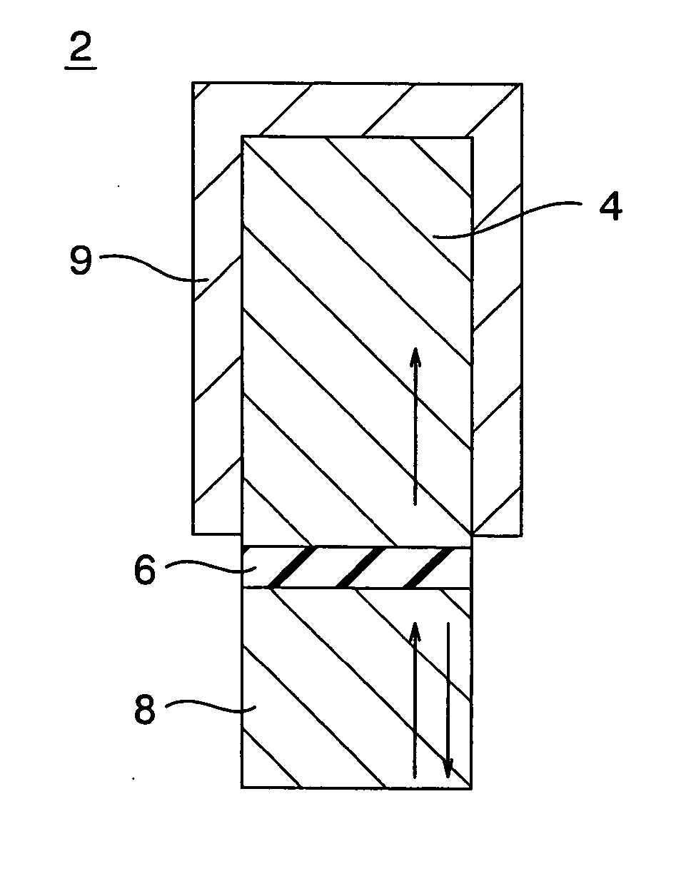
[0062] A constitution of a magneto-resistive effect element according to a first embodiment of the present invention is shown in FIG. 1. The magneto-resistive effect element 2 according to this embodiment is a TMR element, and comprises a magnetization-pinned layer (to be also referred to as a pinned layer hereinafter) 4 having a perpendicular spin moment, a magnetization free layer (to be also referred to as a free layer hereinafter) 8 having a perpendicular spin moment and serving as a magnetic recording layer, a tunnel barrier layer 6 provided between the magnetization-pinned layer 4 and the magnetization free layer 8, and an anti-ferromagnetic film 9 covering side surfaces of the magnetization-pinned layer 4 and a surface of the magnetization-pinned layer 4 opposing the tunnel barrier layer 6.

[0063] In this manner, in the magneto-resistive effect element according to the embodiment, the anti-ferromagnetic film 9 is formed on at least side surfaces of th...

second embodiment

[0064] (Second Embodiment)

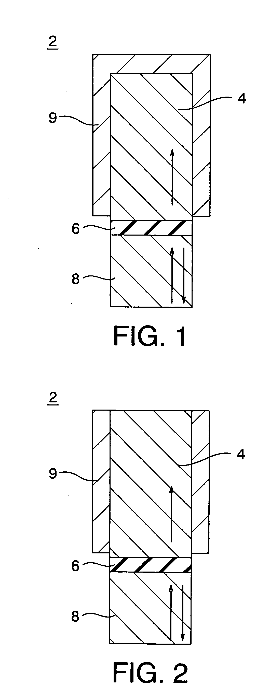
[0065] A constitution of a magneto-resistive effect element according to a second embodiment of the present invention is shown in FIG. 2. The magneto-resistive effect element 2 according to the embodiment has a constitution obtained by removing the anti-ferromagnetic film 9 on the surface of the magnetization-pinned layer 4 opposing the tunnel barrier layer 6 from the magneto-resistive effect element 2 according to the first embodiment shown in FIG. 1, i.e., forming the anti-ferromagnetic film 9 only on the side surfaces of the magnetization-pinned layer 4.

[0066] For this reason, even though the magneto-resistive effect element is miniaturized, the spin moment direction of the magnetization-pinned layer 4 is perpendicularly oriented by exchange coupling between the anti-ferromagnetic film 9 and the magnetization-pinned layer 4. Even though switching of the magnetic fields is repeated, the magnetic domain of the magnetization-pinned layer 4 does not vary. T...

third embodiment

[0067] (Third Embodiment)

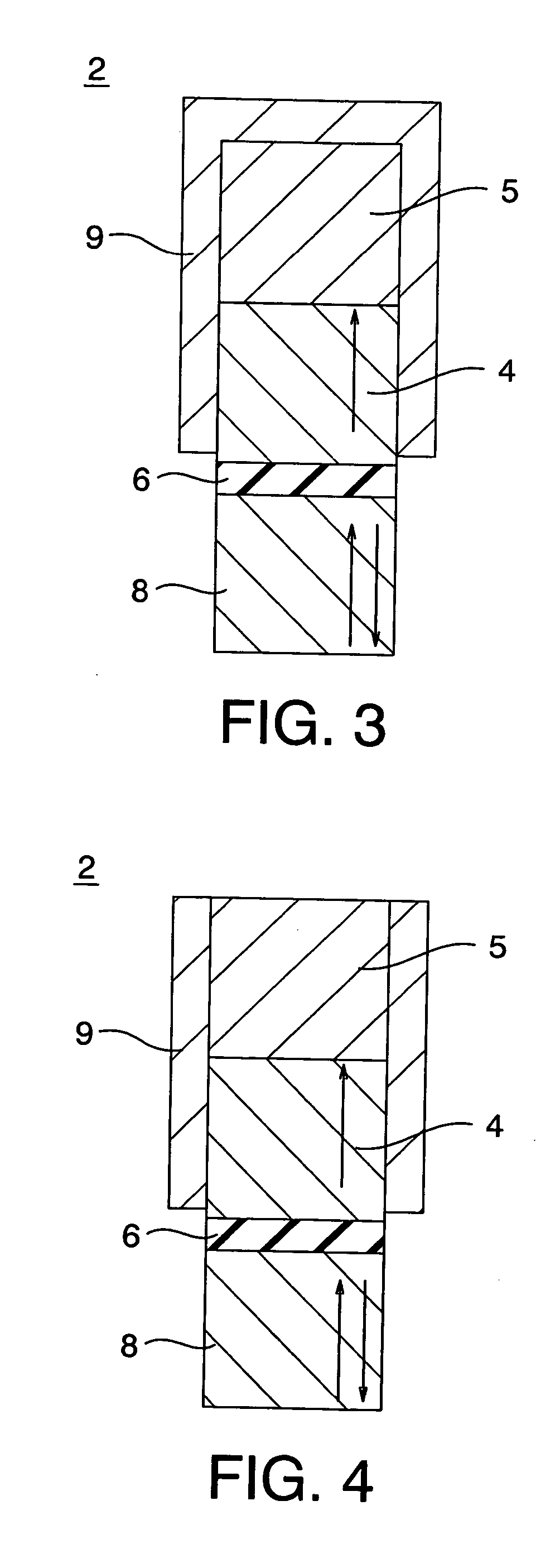
[0068] A constitution of a magneto-resistive effect element according to a third embodiment of the present invention is shown in FIG. 3. The magneto-resistive effect element 2 according to the embodiment has a constitution obtained by forming a nonmagnetic conductive layer 5 on the upper surface of the magnetization-pinned layer 4 in the magneto-resistive effect element 2 according to the first embodiment shown in FIG. 1.

[0069] In the magneto-resistive effect element according to the embodiment, the anti-ferromagnetic film 9 is formed on at least side surfaces of the magnetization-pinned layer 4. Therefore, the spin moment of the magnetization-pinned layer 4 is perpendicularly oriented by exchange coupling between the magnetization-pinned layer 4 and the anti-ferromagnetic film 9 even though the magneto-resistive effect element is miniaturized, and the magnetization of the magnetization-pinned layer 4 does not vary even though switching of the magnetic fiel...


PUM

PropertyMeasurementUnit
thicknessaaaaaaaaaa
thicknessaaaaaaaaaa
thicknessaaaaaaaaaa

Abstract

It is possible to obtain excellent heat stability even though the element is miniaturized and keep stable magnetic domains even though switching is repeated any number of times. A magneto-resistive effect element includes: a magnetization-pinned layer including a magnetic film having a spin moment oriented in a direction perpendicular to a film surface thereof and pinned in the direction; a magnetic recording layer having a spin moment oriented in a direction perpendicular to a film surface thereof; a nonmagnetic layer formed between the magnetization-pinned layer and the magnetic recording layer; and an anti-ferromagnetic film formed on at least side surfaces of the magnetization-pinned layer.

Description

CROSS-REFERENCE TO RELATED APPLICATION [0001] This application is based upon and claims the benefit of priority from prior Japanese Patent Application No. 2003-194513, filed on Jul. 9, 2003 in Japan, the entire contents of which are incorporated herein by reference. BACKGROUND OF THE INVENTION [0002] 1. Field of the Invention [0003] The present invention relates to a magneto-resistive effect element and a magnetic memory. [0004] 2. Related Art [0005] A magneto-resistive effect element having magnetic films is used for a magnetic head, a magnetic sensor and so forth, and it has been proposed to be used for a solid magnetic memory. In particular, there is an increasing interest in a magnetic random access memory (hereinafter, referred to as “MRAM (Magnetic Random Access Memory)), which utilizes the magneto-resistive effect of ferromagnetic material, as a next generation solid non-volatile memory capable of carrying out a rapid reading / writing and an operation with large capacity and l...

Claims


Application Information

Patent Timeline
Patent Type & Authority Applications(United States)
IPC IPC(8): G11C11/16G11C11/15G11C11/22H01F10/14H01F10/16H01F10/32H01L21/8246H01L27/105H01L43/08H01L43/10
CPCG11C11/16H01L43/08H01L27/228H10B61/22H10N50/10
Inventor SAITO, YOSHIAKI
Owner KK TOSHIBA
Why Eureka
Try Eureka