Substrate processing method and substrate processing apparatus

a substrate processing and substrate technology, applied in the field of microwave plasma processing apparatuses, can solve the problems of increasing the overall size of the substrate processing apparatus b>1/b> inevitably, affecting the effect of substrate nitridation, avoiding excessive plasma energy increase, and reducing plasma energy

Inactive Publication Date: 2005-02-24
OHMI +1
View PDF8 Cites 13 Cited by
  • Summary
  • Abstract
  • Description
  • Claims
  • Application Information

AI Technical Summary

Benefits of technology

Accordingly, it is a general object of the present invention to provide a novel and useful substrate processing apparatus wherein the foregoing problems are eliminated.
Another and more specific object of the present invention is to provide a substrate processing method and apparatus capable of forming nitrogen radicals N* efficiently.
According to the present invention, it becomes possible to form plasma having the energy sufficient for causing excitation of atomic state nitrogen N* in the substrate processing apparatus by using He for the plasma excitation gas, and it becomes possible to conduct an efficient nitridation of the substrate by using the atomic state nitrogen N* thus excited. By separating the plasma excitation space in which the high-density plasma is excited from the process space in which the substrate is included by means of the control electrode, it becomes possible to reduce the plasma energy in the process space to the level suitable for substrate processing. Further, it becomes possible to trap the positive ions formed in the plasma excitation space. In the case of applying the present invention to the substrate processing apparatus that uses microwave-excited plasma, it becomes possible to avoid excessive increase of the plasma energy by conducting the plasma excitation by using a microwave having the frequency of about 28 GHz or more.

Problems solved by technology

In such a conventional induction-coupled plasma processing apparatus 1, on the other hand, there exists a drawback in that the high-density plasma 2D is localized at the top part of the processing vessel and there appears an extremely non-uniform distribution in the radicals that are formed with the plasma.
As a result of such a construction, on the other hand, the overall size of the substrate processing apparatus 1 is increased inevitably.
These problems become particularly serious in the technology of current trend of processing a large-diameter substrate.
This means that it is not possible to excite the atomic state nitrogen N* according to the foregoing reaction, as long as Kr or Ar plasma is used.
Such a plasma cannot achieve efficient excitation of the desired nitrogen radicals.

Method used


Image

  • Substrate processing method and substrate processing apparatus
  • Substrate processing method and substrate processing apparatus
  • Substrate processing method and substrate processing apparatus

Examples


first embodiment

[First Embodiment]

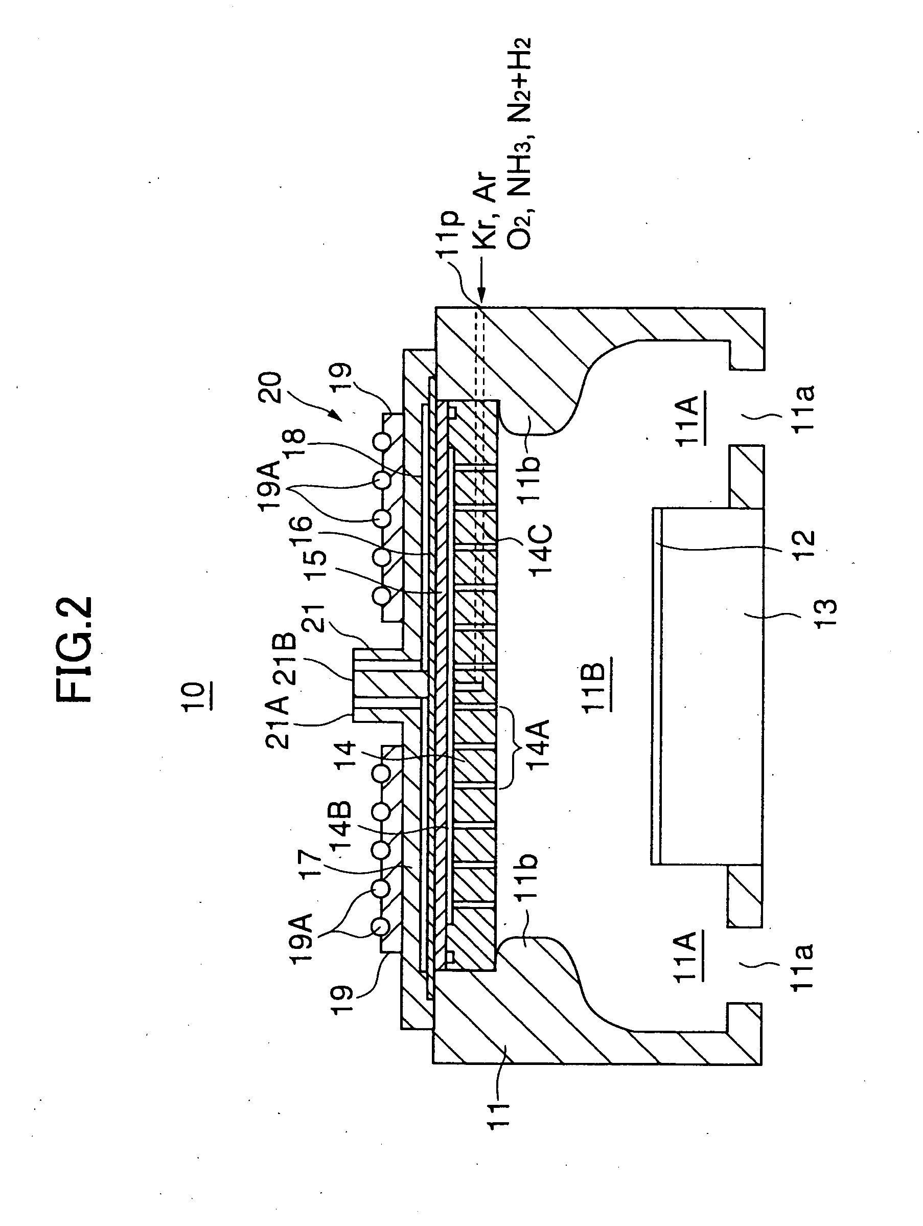
FIG. 5 shows the construction of a substrate processing apparatus 100 according to a first embodiment of the present invention. In FIG. 5, those parts corresponding to the parts described previously are designated by the same reference numerals and the description thereof will be omitted.

Referring to FIG. 5, the shower plate 14 is mounted on the processing vessel 11 via a seal 11s, and the cover plate 15 is mounted on the shower plate 14 via a seal 11t. Further, the radial line slot antenna 20 is mounted on the processing vessel 11 via a seal 11u.

Further, in the substrate processing apparatus 100 of FIG. 5, the interface between the emission plate 16 and the cover plate 15 is evacuated via a ring-shaped groove 11g formed at the top part of the processing vessel 11 in the region where the processing vessel makes an engagement with the emission plate and further via an evacuation port 11G communicating with the ring-shaped groove 11g. After evacuation, a He gas i...

second embodiment

[Second Embodiment]

FIG. 9 shows the construction of a substrate processing apparatus 200 according to a second embodiment of the present invention. In FIG. 9, those parts corresponding to the parts described previously are designated by the same reference numerals and the description thereof will be omitted.

Referring to FIG. 9, it should be noted that the shower plate 14 is removed in the present embodiment, and in place of this, there are provided a plurality of process gas inlet ports lip on the processing vessel 11 such that the process gas inlet ports 11P are disposed with a symmetric relationship with respect to the substrate 12. As a result, therefore, the cover plate 15 constituting the dielectric window is exposed at the top part of the plasma excitation space 11B. Further, the sidewall surface of the processing vessel is covered by the quartz liner 11D for the part corresponding to the plasma excitation space 11B similarly to the previous embodiment.

According to the pre...

third embodiment

[Third Embodiment]

FIG. 10 shows the construction of a substrate processing apparatus 300 according to a third embodiment of the present invention. In FIG. 10, those parts corresponding to the parts described previously are designated by the same reference numerals and the description thereof will be omitted.

Referring to FIG. 10, the substrate processing apparatus 300 has a construction similar to the substrate processing apparatus 1 explained before with reference to FIG. 1, except that a control electrode 6 similar to the control electrode 31 is provided in the quartz vessel 2, and the space inside the quartz vessel 2 is divided by the control electrode 6 into a plasma excitation space 2B1 in which the high-density plasma 2D is excited and a process space 2B2 that includes the substrate 4 to be processed.

In the present embodiment, a He gas and an N2 gas are introduced into the plasma excitation space 2B1 via the process gas supply line 2C, and there is formed high-density plasm...


PUM

PropertyMeasurementUnit
energyaaaaaaaaaa
gate lengthaaaaaaaaaa
energyaaaaaaaaaa

Abstract

In a substrate processing apparatus, a control electrode (131) separates a process space (11C) including a substrate to be processed and a plasma formation space (11B) not including the substrate. The control electrode includes a conductive member formed in a processing vessel and having a plurality of apertures (131a) for passing plasma. A surface of the control electrode is covered by an aluminum oxide or a conductive nitride. In the substrate processing apparatus, a gas containing He and N2 is supplied into the processing vessel. In the plasma formation space, there is formed plasma under a condition in which atomic state nitrogen N* are excited. The atomic state nitrogen N* are used to nitride a surface of the substrate.

Description

TECHNICAL FIELD The present invention generally relates to plasma processing apparatuses and more particularly to a microwave plasma processing apparatus. Plasma process and plasma processing apparatus constitute indispensable technology for fabricating ultrafine semiconductor devices such as the one called deep submicron device or deep sub-quarter micron device having a gate length near 0.1 μm or less, or for fabricating high-resolution flat panel display device including a liquid crystal display device. Conventionally, various plasma excitation methods have been employed in the plasma processing apparatus used for fabricating semiconductor devices or liquid crystal display devices. Particularly, high-frequency plasma apparatuses of parallel plate type or induction-coupled type plasma apparatus are used commonly. However, such a conventional plasma processing apparatuses suffers from the problem of non-uniform plasma formation in that the region in which high electron density is...

Claims


Application Information

Patent Timeline
Patent Type & Authority Applications(United States)
IPC IPC(8): C23C8/36C23C16/02C23C16/56C23C16/511H01J37/32H01L21/31H01L21/314H01L21/318
CPCC23C8/36H01J37/321H01L21/318H01L21/3143H01J37/32357H01L21/02247H01L21/02252
Inventor OHMI, TADAHIROHIRAYAMA, MASAKI
Owner OHMI
Why Eureka
Try Eureka