In the process, it is, however, to be observed as an unpleasant
side effect that already the housing and mounting of the integrated circuitry in a housing imparts a substantial mechanical stress onto the semiconductor material and thus to the semiconductor substrate of the integrated circuitry.
As the semiconductor material of the integrated circuitry and the plastic
casting compound material of the housing surrounding the integrated circuitry comprise non-matching thermal coefficients of expansion, the plastic material contracts more strongly when cooling to ambient temperature (
room temperature) and therefore exerts a mechanical stress onto the semiconductor material of the integrated circuitry which is hard to predict and therefore not very well reproducible.
It thus becomes clear that with an exceedingly high mechanical stress, the electric functioning of the integrated circuitry may be affected, wherein initially generally only the electronic performance of the integrated circuitry will decrease.
This decrease of the performance is for example to be observed in the form of an impairment of the modulation range, the resolution, the
band width, the
current consumption, the accuracy, etc., wherein it is to be considered that with a higher mechanical stress in the semiconductor material a partial or also complete functioning failure of the integrated circuitry may result which is generally still reversible, however.
With an even further
increased stress in the semiconductor material finally a crack formation in the semiconductor material will occur, wherein the
semiconductor chip may finally break so that an irreversible damage of the integrated circuitry will occur.
The caused mechanical stress may negatively influence the performance of both analogue and digital circuits or may also lead to a complete failure of the integrated circuitry.
As the mechanical stresses are generally not well reproducible at an integrated circuitry in a semiconductor material, as they depend on the combination of the used materials and the
processing parameters, like e.g. solidification temperature and solidification time of the compound
mass of the housing of the
integrated circuit, a unique characterization of any concerned parameters may generally not lead to the desired aim in the laboratory.
Performance impairments occur, however, very product-specifically and may therefore not always be considered sufficiently in housing development.
Because these changes may concern many different products, however, in this case the post-qualifications are generally only performed on selected IC groups exemplary for the whole IC
product family.
The diverse influence possibilities of mechanical stress onto the functioning of a highly integrated circuitry are manifold, however, and are not easily apparent, so that it frequently occurs that with such a change the characteristics of a product become worse due to one of the above effects.
Particularly problematic is the above-explained problem with automotive products, i.e. products for the vehicle area, as these products are frequently subject to extreme temperatures or temperature fluctuations, respectively, but in case of sensors for security systems, like for example ABS sensors,
airbag sensors, etc., have to function in a highly reliable way over their complete life.
From this group of products the automotive sensors are also very prone to piezo-interactions, as these automotive sensors are frequently subjected to specially extreme temperatures due to their use and need to work a lot more accurately as sensors in security systems than it is the case with simple digital integrated circuitries.
The above-discussed problem is, however, even further increased when the integrated circuitries housed in a housing are again assembled in a module.
When
casting, again substantial mechanical stresses may be caused in the semiconductor material of the integrated circuitry.
It is, however, generally not possible with a reasonable technical effort to keep the manufacturing parameters of those
processing sequences sufficiently reproducible, so that also in the course of the production of the above-mentioned module substantial fluctuations of the mechanical stresses in the semiconductor material of the integrated circuitries on the
semiconductor chip may result.
As the modules already comprise a considerable
mass, generally several 100 grams, it is further not possible basically due to the very high technical effort and therefore for cost reasons, to test all manufactured modules at the minimal
operation temperature with regard to the problem regarding piezo-effects at the output of the
manufacturing line.
Due to the considerable
mass of for example several 100 grams, a relatively long time period would be required in order to cool every module completely to the minimal
operation temperature.
Apart from that, generally during the production of the modules, an attempt is made not to apply temperatures below
dew point, as thereby
condensed water may result and the same may cause leakage currents in exact
electrical measurements.
Accompanying the manufacturing, both at the semiconductor manufacturer and at the module manufacturer sample tests are performed, as it would be extremely cost- and time-consuming to perform corresponding functioning tests on all completed semiconductor devices or modules, respectively.
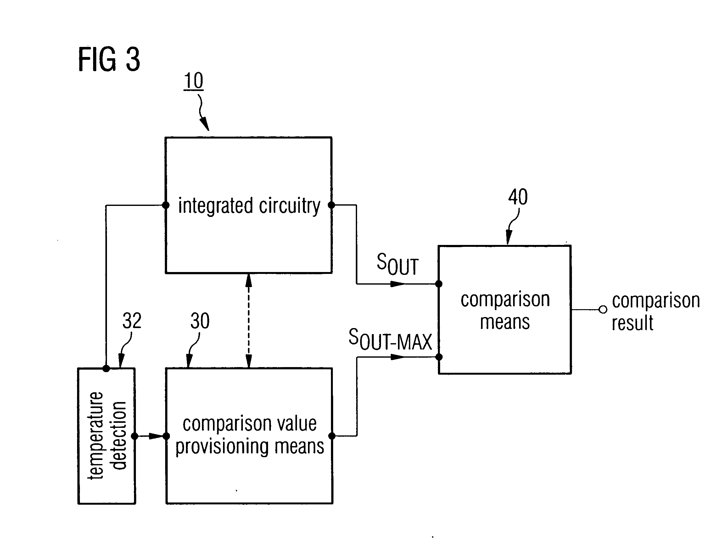
As mechanical stresses in the semiconductor material of an integrated circuitry were found to be a reliability risk, it was now started to monitor the mechanical stress.
This may for example be performed in
semiconductor chip manufacturing, wherein it is generally not possible, however, to perform such cost- and time-consuming electronic tests after the manufacturing of the module, as the integrated circuitry (IC) is already located in a
complex system with numerous other components and is not individually acceptable any more.
Additionally, piezo-effects may spread to a
system in hardly (or not at all) predictable ways and generate detrimental effects.
In particular, mechanical stresses in a semiconductor
chip may only cause relatively small
observable changes in the integrated circuitry, wherein, however, in connection with other
system components, a failure or a performance decrease of the integrated circuitry or the circuit module, respectively, may then result.
Due to the occurring non-linearities of the used circuit structures this is, however, mainly not sufficiently possible.
In addition it is to be noted, that such temperature derivative actions are also again flawed with tolerances.
From the above disclosures it becomes clear that it is very cost and
time consuming in
chip or module manufacturing, respectively, to examine the functioning of all integrated circuitries accommodated in a housing or module, respectively, with regard to the influence of mechanical stresses in the semiconductor material.
In the
simulation of the mechanical stress values in the semiconductor material of an integrated circuitry, which is provided to make predictions with regard to the functioning of the circuitry and to be able to suitably adapt the
circuit design of the same, it should be considered, however, that already slight changes of the housing materials, the manufacturing sequence or of individual
processing steps may invalidate the practicality and the use of the simulated values.

