
Semiconductor device, method of fabricating same, and electrooptical device

a semiconductor and thin-film technology, applied in the field of semiconductor devices, can solve problems such as difficulty in forming thin-film transistors, and achieve the effect of suppressing drawbacks

Inactive Publication Date: 2005-03-03
PATENT TREUHAND GESELLSCHAFT FUR ELECTRIC GLUEHLAMPEN MBH
View PDF99 Cites 7 Cited by
  • Summary
  • Abstract
  • Description
  • Claims
  • Application Information

AI Technical Summary

Benefits of technology

[0015] In the above-described structure, the resinous layer acts to planarize the surface of the resinous substrate. The planarization also serves to prevent precipitation of oligomers on the surface of the resinous substrate during steps involving heating such as the step for forming the semiconductor layer.
[0016] The material of this resinous layer can be selected from methyl esters of acrylic acid, ethyl esters of acrylic acid, butyl esters of acrylic acid, and 2-ethylhexyl esters of acrylic acid. Even if resinous substrates are used, this resinous layer can suppress the drawbacks with fabrication of the afore-mentioned thin-film transistors.
[0019] In the above-described structure, heat-treatment is made to degas the resinous substrate, in order to prevent escape of gases from the resinous substrate during later processes involving heating. For example, if gases are released from the resinous substrate when a semiconductor thin film is being formed on the resinous substrate, then large pinholes are formed in the semiconductor thin film. This greatly impairs the electrical characteristics. Accordingly, the substrate is heat-treated at a temperature higher than heating temperatures used in the later processes, to degas the resinous substrate. In this way, release of gases from the resinous substrate during the later steps can be suppressed.

Problems solved by technology

However, because of poor heat resistance of resinous substrates, it is technically difficult to form thin-film transistors on them.

Method used


Image

  • Semiconductor device, method of fabricating same, and electrooptical device
  • Semiconductor device, method of fabricating same, and electrooptical device
  • Semiconductor device, method of fabricating same, and electrooptical device

Examples


example 1

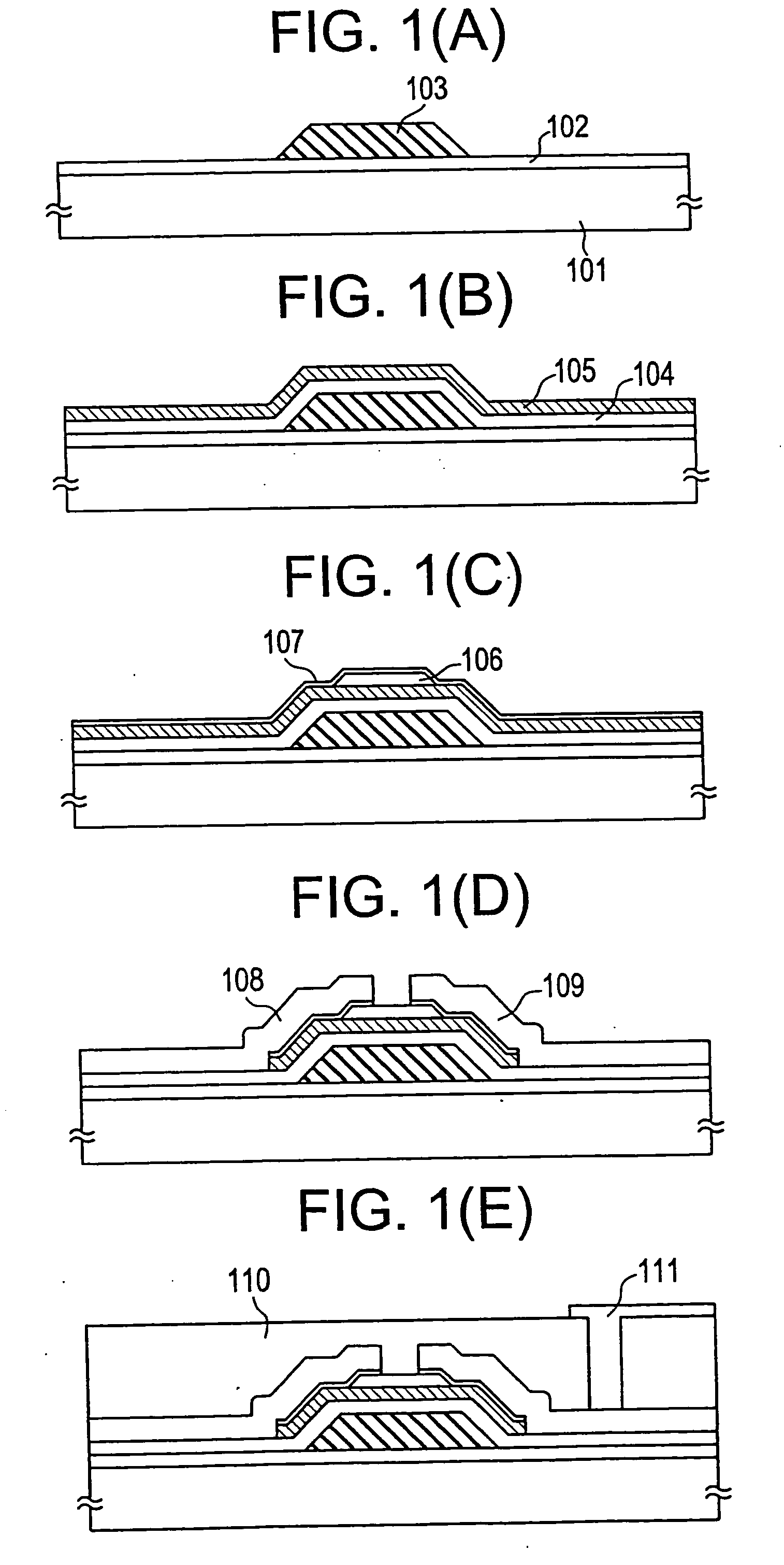
[0027] The present example shows an example in which inverted-staggered TFTs are formed on a substrate of PET (polyethylene terephthalate) which is an organic resin.

[0028] As shown in FIG. 1(A), a PET film 101 having a thickness of 100 μm is first prepared and heat-treated to degas the film. This heat-treatment is required to be conducted at a temperature higher than the highest temperature applied in later processes. In the processes shown in the present example, a temperature of 160° C. used during formation of an amorphous silicon film by plasma-assisted CVD is the highest heating temperature. Therefore, the heat-treatment for degassing the PET film is performed at 180° C.

[0029] A layer of an acrylic resin 102 is formed on this PET film 101. As an example, a methyl ester of acrylic acid can be used as the acrylic resin. This acrylic resin layer 102 acts to prevent precipitation of oligomers on the surface of the PET film 101 in processes conducted later. The acrylic resin layer...

example 2

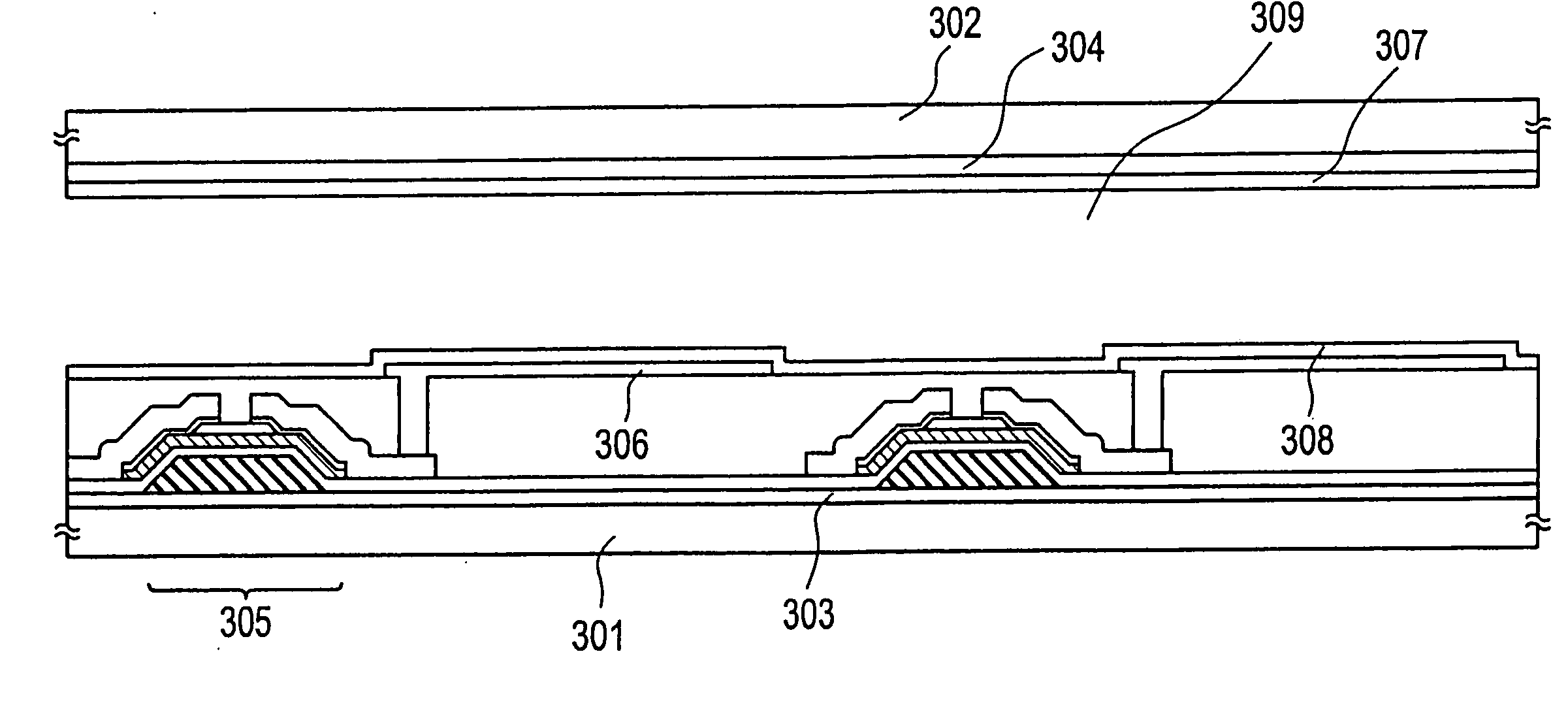
[0038] The present example shows a case in which an active matrix liquid crystal display is fabricated, using the thin-film transistors described in Example 1. The liquid crystal electrooptical device described in the present example is shown in FIG. 3 in cross section.

[0039] In FIG. 3, PET films 301 and 302 having a thickness of 100 μm form a pair of substrates. An acrylic resin layer 303 acts as a planarizing layer. Indicated by 306 are pixel electrodes. In FIG. 3, only the structure corresponding to two pixels is shown.

[0040] Indicated by 304 is a counter electrode. Orientation films 307 and 308 orient a liquid crystal 309 which can be a twisted-nematic (TN) liquid crystal, supertwisted-nematic (STN) liquid crystal, or a ferroelectric liquid crystal. Generally, a TN liquid crystal is employed. The thickness of the liquid crystal layer is several micrometers to about 10 μM.

[0041] Thin-film transistors (TFTs) 305 are connected with the pixel electrodes 306. Electric charge going...

example 3

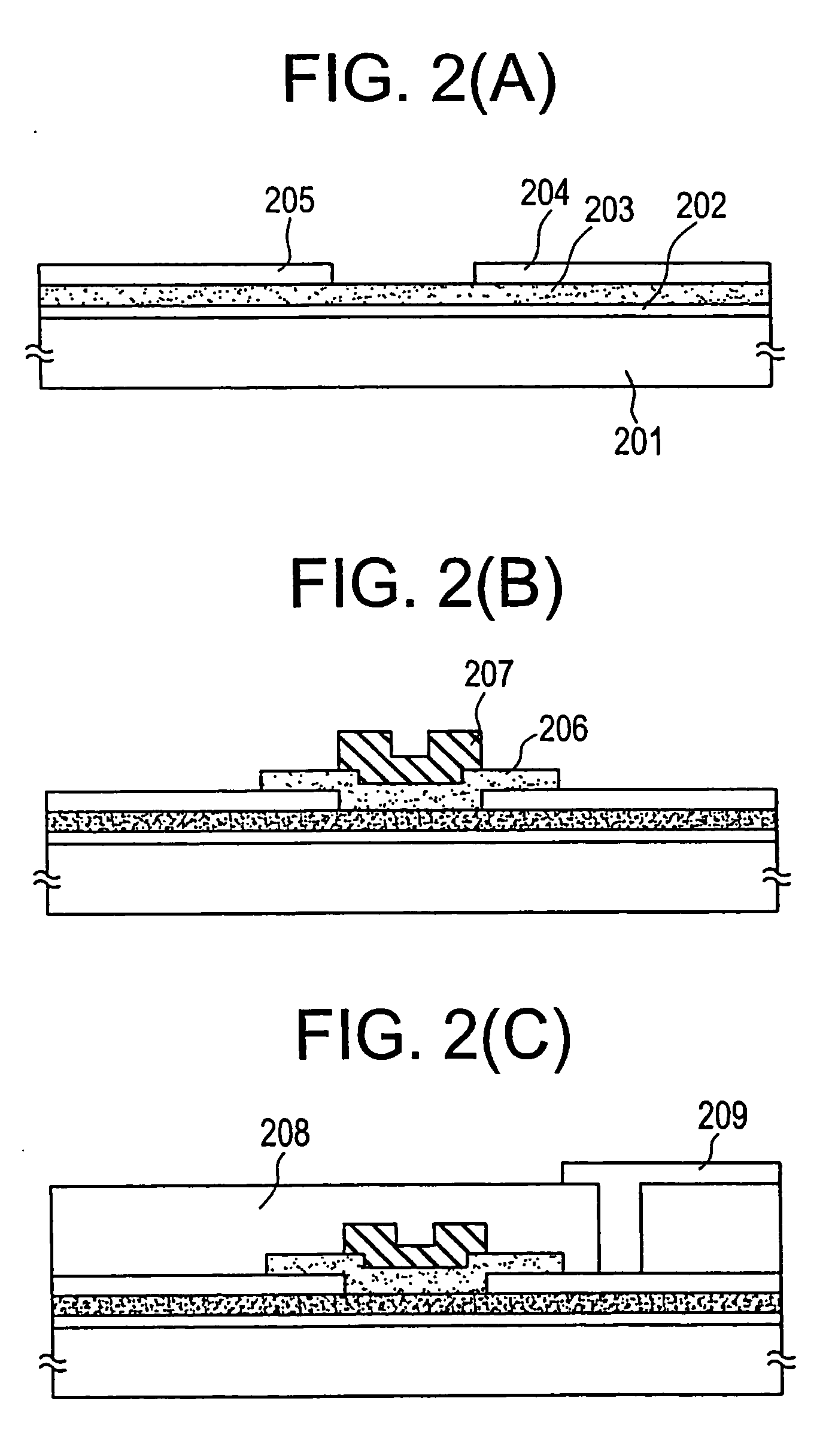
[0043] The present example shows an example in which coplanar thin-film transistors used for an active matrix liquid crystal display are fabricated. The process sequence for fabricating the thin-film transistors of the present example is shown in FIG. 2. First, a PET film 201 having a thickness of 100 μm is prepared as a filmy organic resin substrate. The film is heated-treated at 180° C. to promote degassing from the PET film 201. A layer of an acrylic resin 202 is formed on the surface of the film. In this example, an ethyl ester of acrylic acid is used as the acrylic resin.

[0044] Then, a substantially intrinsic (I-type) semiconductor layer 203 in which a channel formation region is formed is grown by plasma-assisted CVD under the following conditions:

film formation temperature160° C.(at which the substrate is heated):reaction pressure:0.5 torrRF power (13.56 MHz):20 mW / cm2reactant gas:SiH4

[0045] In this example, a parallel-plate plasma-CVD machine is used to grow the film.

[00...


PUM

PropertyMeasurementUnit
thicknessaaaaaaaaaa
diametersaaaaaaaaaa
temperatureaaaaaaaaaa

Abstract

A pair of substrates forming the active matrix liquid crystal display are fabricated from resinous substrates having transparency and flexibility. A thin-film transistor has a semiconductor film formed on a resinous layer formed on one resinous substrate. The resinous layer is formed to prevent generation of oligomers on the surface of the resinous substrate during formation of the film and to planarize the surface of the resinous substrate.

Description

BACKGROUND OF THE INVENTION [0001] 1. Field of the Invention [0002] The present invention relates to a configuration of thin-film transistors (TFTs) formed on a flexible substrate (i.e., having mechanical flexibility) such as a resinous substrate which can be made of engineering plastics. The invention also relates to a method of fabricating such thin-film transistors. Furthermore, the invention relates to an active matrix liquid crystal display fabricated, using these thin-film transistors. [0003] 2. Prior Art [0004] Thin-film transistors formed on glass substrates or on quartz substrates are known. Thin-film transistors formed on glass substrates are chiefly used in active matrix liquid crystal displays. Since active matrix liquid crystal displays can display images with high response and with high information content, it is expected that they can supplant simple matrix liquid crystal displays. [0005] In an active matrix liquid crystal display, one or more thin-film transistors ar...

Claims


Application Information

Patent Timeline
Patent Type & Authority Applications(United States)
IPC IPC(8): G02F1/136G02F1/13G02F1/1333G02F1/1362G02F1/1368H01L21/00H01L21/84H01L29/78H01L29/786
CPCG02F1/133305H01L29/78636G02F1/136227H01L29/786
Inventor YAMAZAKI, SHUNPEIARAI, YASUYUKITERAMOTO, SATOSHI
Owner PATENT TREUHAND GESELLSCHAFT FUR ELECTRIC GLUEHLAMPEN MBH
Learn More