Method of acquiring low distortion and high linear characteristic in triode-typed transconductor
a triode-type transconductor and high-linear characteristic technology, applied in the field of transconductor, can solve the problems of large area consumption, unsuitability, complex circuit, etc., and achieve the effect of low distortion, constant, and high linearity
- Summary
- Abstract
- Description
- Claims
- Application Information
AI Technical Summary
Benefits of technology
Problems solved by technology
Method used
Image
Examples
first embodiment
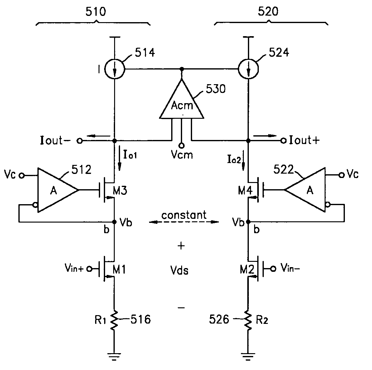
FIG. 7 is a circuit diagram illustrating the triode-typed transconductor according to the present invention.
Referring to FIG. 7, the transconductor includes a first transconductor circuit 510 and a second transconductor circuit 520. A common mode amplifier 530 is disposed between the first transconductor circuit 510 and the second transconductor circuit 520 so as to maintain a common mode that makes output DC voltage constant. The common mode amplifier 530 has a common mode gain (Acm), and includes a common mode voltage (Vcm) input terminal for comparing the common mode to differential outputs each other. An output terminal Iout− of the first transconductor circuit 510 that is connected to the common mode amplifier 530 maintains the common mode by the common mode amplifier 530. Also, an output terminal Iout+ of the second transconductor circuit 520 that is connected to the common mode amplifier 530 maintains the common mode.
The first transconductor circuit 510 includes a first me...
second embodiment
FIG. 8 is a circuit diagram illustrating the triode-typed transconductor according to the present invention. In FIG. 8, same reference numerals as those of FIG. 7 denote same elements. Thus, descriptions for the same elements as those of FIG. 7 will be omitted.
As shown in FIG. 8, the transconductor of the present embodiment is different in that an active resistance device realized by the MOS is used unlike the first embodiment, in which the passive resistor is used. That is, a first active resistance device 518 is disposed between the source terminal and the grounded terminal of the first MOS transistor M1 in the first transconductor circuit 510. Also, a second active resistance device 528 is disposed between the source terminal and the grounded terminal of the second MOS transistor M2 in the second transconductor circuit 520. The first active resistance device 518 and the second active resistance device 528 are fabricated using MOS transistors. A drain terminal of the first active...
third embodiment
FIG. 9 is a circuit diagram illustrating the triode-typed transconductor according to the present invention.
Referring to FIG. 9, the transconductor of the third embodiment includes a first transconductor circuit 610 and a second transconductor circuit 620. A common mode amplifier 630 is disposed between the first transconductor circuit 610 and the second transconductor circuit 620. The common mode amplifier 630 has a common mode gain Acm, and includes a common mode voltage Vcm input terminal. An output terminal Iout− of the first transconductor circuit 610, which is connected to the common mode amplifier 630, maintains the common mode by the common mode amplifier 630. Also, an output terminal Iout+ of the second transconductor 620, which is connected to the common mode amplifier 630, maintains the common mode.
The first transconductor circuit 610 includes the first MOS transistor M1, the third MOS transistor M3, a first amplifier 612 that constructs a regulator cascode circuit, a ...
PUM
 Abstract
Description
Claims
Application Information


