Light-emitting apparatus and fabrication method of the same

a technology of light-emitting apparatus and fabrication method, which is applied in the manufacture of electric discharge tubes/lamps, discharge tubes luminescnet screens, electrode systems, etc., can solve the problems of easy damage to the electrostatic discharge surface, threat of dust adhesion to the charged surface or generating electrostatic discharge, and poor coverage. , to achieve the effect of preventing electrostatic discharge damag

Inactive Publication Date: 2005-03-17
SEMICON ENERGY LAB CO LTD
View PDF45 Cites 125 Cited by
  • Summary
  • Abstract
  • Description
  • Claims
  • Application Information

AI Technical Summary

Benefits of technology

[0036] An electrostatic discharge damage can be prevented by forming an antistatic layer that covers an insulting film that serves as a second bank. The another structure relating to a fabrication method according to the present invention is that a fabrication method for a light-emitting apparatus including a light-emitting device having a first electrode, an organic compound layer, and a second electrode over a substrate having an insulating surface, comprising steps of forming a TFT and the first electrode over the substrate and forming a lamination layer of an organic resin film or an inorganic insulating film and an antistatic layer with covering the first electrode over a whole surface at a first installation site, transporting a substrate into a second installation site, etching the antistatic layer, forming a bank by etching the organic resin film or the inorganic insulating film, and forming the organic compound layer over the first electrode without exposing to the air after exposing a part of the first electrode at the second i

Problems solved by technology

In case of separating equipment, a problem will arise that substrates should be transported between the installation sites, and there is a risk of electrostatic discharge damage and adhesion of dust on a substrate during transportation of the substrates.
Further, since a substrate, an organic insulating film, and an inorganic insulating film are insulators, static electricity is easily charged a surface thereof, Due to th

Method used


Image

  • Light-emitting apparatus and fabrication method of the same
  • Light-emitting apparatus and fabrication method of the same
  • Light-emitting apparatus and fabrication method of the same

Examples


embodiment

[0065] Embodiment Mode 1

[0066] The present invention is described by using an example of an active matrix light-emitting device in this embodiment mode.

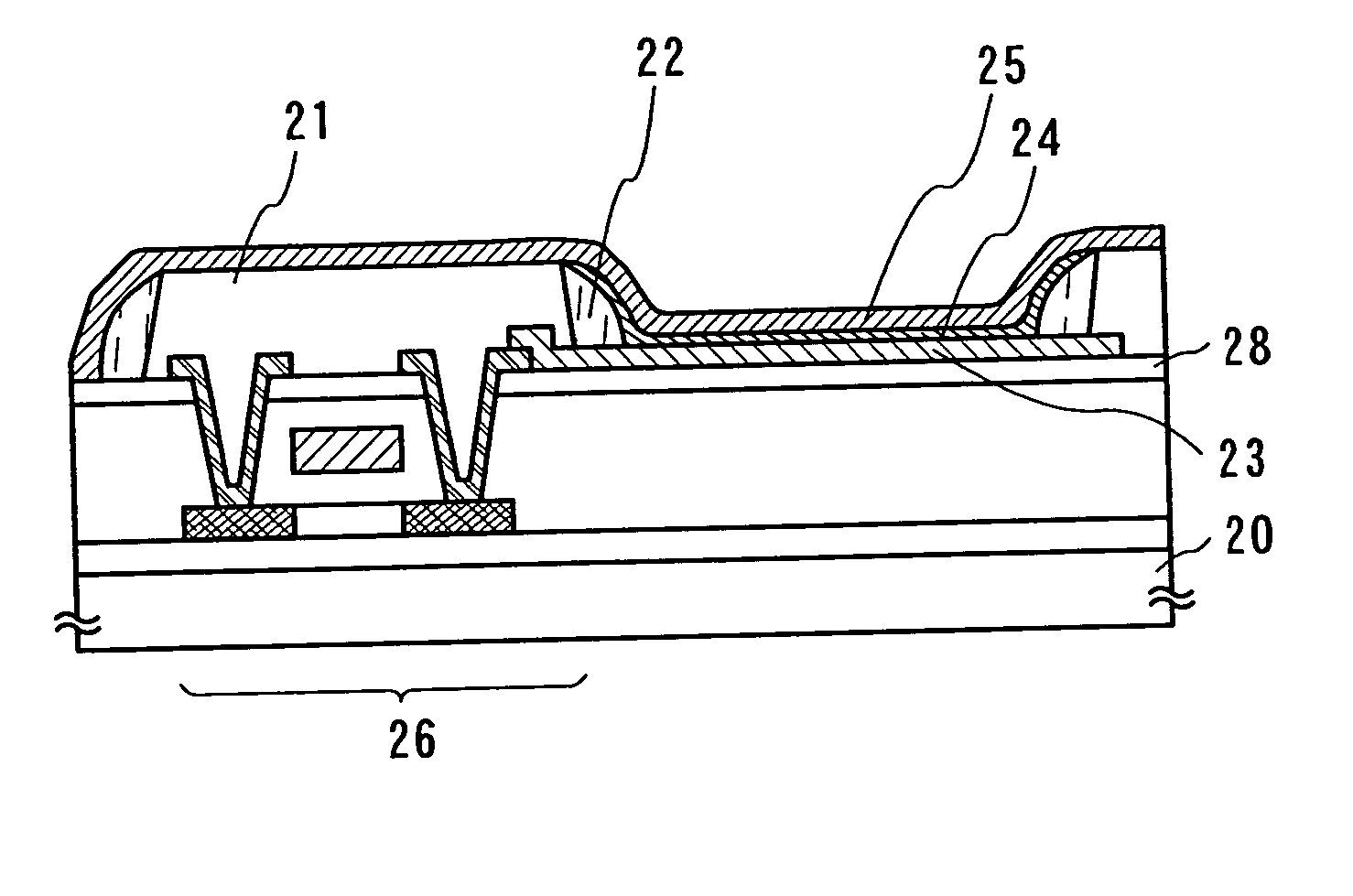
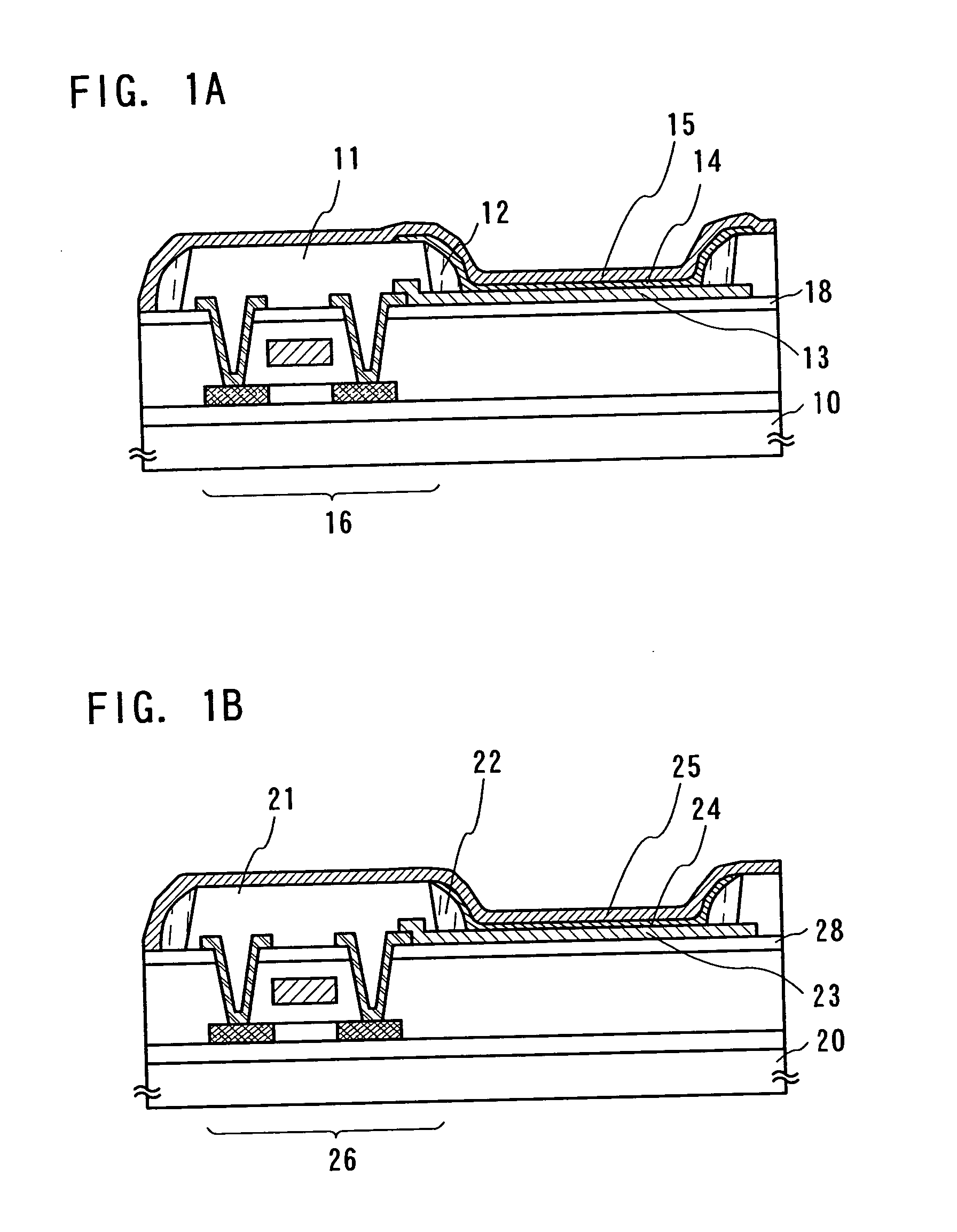
[0067] In FIG. 1A, reference numeral 10 is a substrate, 11 is a first bank, 12 is a second bank, 13 is a first electrode, 14 is an organic compound layer, 15 is a second electrode, 16 is a TFT, and 18 is an insulating film. In FIG. 1A, the electrode 13 serves as an anode of a light-emitting device and the second electrode serves as a cathode of the light-emitting device, but not exclusively, the first electrode can serve as a cathode and the second electrode can serve as an anode if materials are selected appropriately.

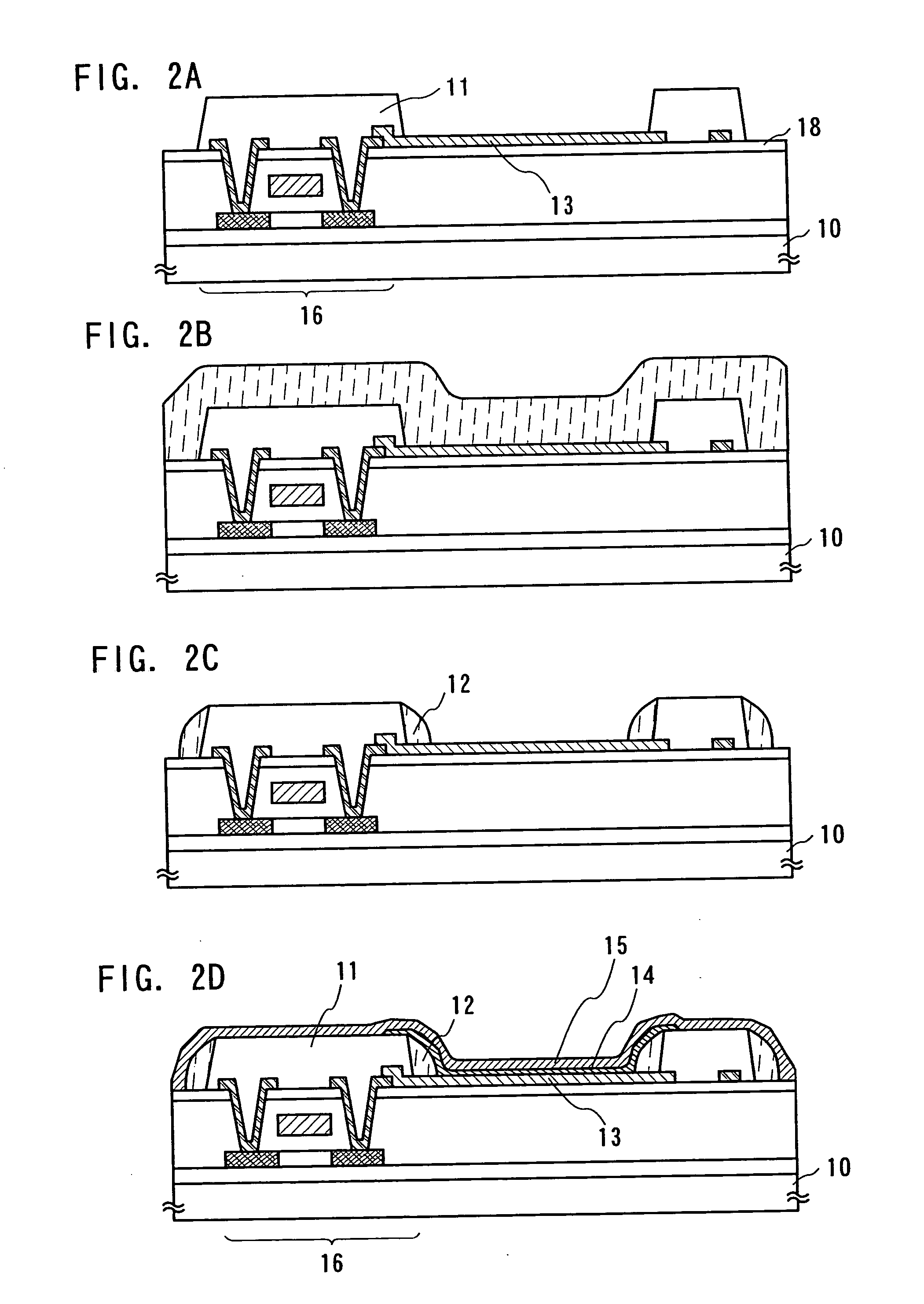
[0068] An example of fabrication process for forming a structure illustrated in FIG. 1A is shown in FIGS. 2A, 2B, 2C and 2D.

[0069] The TFT 16 is fabricated over the substrate 10 having an insulating surface. As materials for an interlayer insulating film of the TFT, for example, inorganic materials formed by sputter...

embodiment 1

[0190] Embodiment 1

[0191]FIGS. 8A and 8B show an example of fabricating a light-emitting apparatus (having a top emitting structure) that includes a light-emitting device having an organic compound layer as a light-emitting layer over a substrate having an insulating surface.

[0192]FIG. 8A is a top view showing the light-emitting apparatus, and FIG. 8B is a cross-sectional view taken along the line A-A′ of FIG. 8A. Reference numeral 1101 indicat d by the dotted line is a source signal line drive circuit; 1102 is a pixel portion; and 1103 is a gate signal line drive circuit. Further, reference numeral 1104 is a transparent sealing substrate; 1105 is a first sealant; and 1107 is a transparent second sealant. An inside area surrounded by the first sealant 1105 is filled with the transparent second sealant 1107. The first sealant 1105 contains a gap material for spacing out the sealing substrate 1104 and the substrate 1110.

[0193] Reference numeral 1108 is a connection wiring for transm...

embodiment 2

[0220] Embodiment 2

[0221] In this embodiment, an example of fabricating such a device that has various functions of materials and a division of function within a lamination structure for improving the mobility of carriers presenting in an organic compound film by relaxation of an energy barrier will be described.

[0222] The technique of inserting a carrier injection layer contributes with respect to the relaxation of the energy barrier in the lamination structure. That is, by inserting a material that relaxes the energy barrier into an interface between the lamination structure having a large energy barrier, the energy barrier can be designed in a staircase pattern. Consequently, a carrier injection property from the electrode can be improved and a driving voltage can be reduced to a certain extent. However, a problem is caused that the number of organic interfaces is increased with increasing the number of layers. That is the reason why a single layer structure rather holds top dat...


PUM


Abstract

Conventionally, there are problems that high resolution is difficult to be achieved since an extreme narrow width bank can not be formed and an aperture ratio as a light-emitting device is low. In addition, there is a threat of electrostatic discharge damage or adhesion of dust during the transportation of a substrate provided with an anode into the equipment for depositing EL material. In view of the foregoing, a first bank formed of an inorganic insulating film is formed, and an insulating film is formed thereon, then, a second bank in contact with a side face of the first bank by carrying out etch back, and then, a side wall bank is formed. For preventing electrostatic discharge damage, an antistatic layer is formed, and the substrate is transported, then, the antistatic layer is removed to form the second bank.

Description

BACKGROUND OF THE INVENTION [0001] 1. Field of the Invention [0002] The present invention relates to a light-emitting apparatus comprising a light-emitting device, which emits fluorescence or phosphoresce upon application of an electric field thereto, including a pair of electrodes and a film containing an organic compound (hereinafter, an organic compound layer) that is sandwiched between the pair of electrodes, and to a method of fabricating the light-emitting apparatus. In this specification, the term light-emitting apparatus includes an image display apparatus, a light-emitting device, or a light source (including a lighting system). Also, the following modules are included in the light-emitting apparatus: a module obtained by attaching a connector such as an FPC (flexible printed circuit), a TAB (tape automated bonding) tape, or a TCP (tape carrier package) to a light-emitting device; a module obtained by providing a PWB (printed wiring board) with a tip of a TAB tape or a TCP;...

Claims


Application Information

Patent Timeline
IPC IPC(8): H01L27/32H05B33/22
CPCH05B33/22H01L27/3246H10K59/122H05B33/10
Inventor KUWABARA, HIDEAKI
Owner SEMICON ENERGY LAB CO LTD
Why Eureka
Try Eureka