Solid state laser using a semiconductor pumping light source

a solid-state laser and semiconductor technology, applied in the direction of laser cooling arrangements, laser details, active medium materials, etc., can solve the problems of laser crystal damage, laser crystal destruction, excessive thermal stress, etc., to achieve the effect of maximizing laser output, increasing tolerance for high-power pumping light, and enhancing the present invention

Inactive Publication Date: 2005-03-17
SHOWA OPTRONICS
View PDF16 Cites 18 Cited by
  • Summary
  • Abstract
  • Description
  • Claims
  • Application Information

AI Technical Summary

Benefits of technology

[0031] That the individual laser crystals are each made of a material having a composition expressed by a same chemical formula means that they consist of a combination of same elements. By thus arranging the individual laser crystals containing varying concentrations of rare earth ions but a same combination of elements, the absorption of laser for each length can be made uniform so that the tolerance for a high power pumping light is increased, and the laser output can be maximized without damaging the laser crystal. In particular, when the laser crystal is provided with a heat sink on side faces thereof for removal of heat, the advantages of the present invention are particularly enhanced.
[0032] When the individual laser crystals are prepared to have different rare earth ion concentrations and to be otherwise similar to one another, the laser crystal can be prepared substantially more economically than a single-piece laser crystal having a continually varying rare earth ion concentration distribution. Also, the multi-piece or composite laser crystal pumped from one end surface simplifies the alignment, and is suitable for mass production.
[0033] When the individual laser crystals are integrally bonded to each other by thermal bonding or other modes of bonding, the alignment and other manufacturing processes as well as stocking of the components are simplified.
[0034] If the individual laser crystals are disposed simply in close mutual contact or the individual laser crystals are spaced from each other by a gap substantially smaller than a length of a shortest one of the individual laser crystals, the manufacturing cost can be minimized.

Problems solved by technology

However, in case of an end pumped or axially pumped solid state laser using a laser diode as a light source, as the output of the light source or the laser diode is increased to increase the laser output, the input end of the laser crystal may be damaged by the incident light.
Also, excessive thermal stress may be caused in the laser crystal because the temperature rise and thermal expansion in the laser crystal is uneven, and this may even destroy the laser crystal.
Therefore, a large part of the energy of the input light is absorbed by the input end of the laser crystal so that the input end of the laser crystal is prone to damages.
Therefore, when a high output laser diode is used as a light source, even if the input light beam is properly shaped, it is difficult to have the input light travel through the laser crystal while maintaining an extremely small beam diameter, and the beam diameter undesirably increases as it travels through the laser crystal.
This in turn causes a higher transverse mode, thereby impairing the beam quality and pumping density.
As a result, a desired efficiency cannot be achieved.
However, this arrangement is not suited for mass production because the axes of the pumping light and output laser are not coaxial and this makes the optical adjustment highly difficult.

Method used


Image

  • Solid state laser using a semiconductor pumping light source
  • Solid state laser using a semiconductor pumping light source
  • Solid state laser using a semiconductor pumping light source

Examples


first embodiment

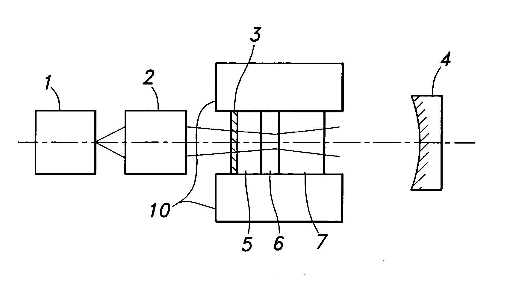
[0049]FIG. 1 shows a first embodiment of the present invention in the form of a laser diode pumped solid state laser. The pumping source of this laser consists of a laser diode 1 having a continuous output of 40 W at 809 nm, and has a light emitting area which is 10 mm wide and 1 μm high. The output of this laser diode is focused by an optical assembly 2 similar to that disclosed in U.S. Pat. No. 5,805,748 into a beam of 600 μm square.

[0050] The first laser crystal 5 consists of a Nd:YVO4 crystal having a Nd3+ concentration of 0.25 atomic % and 0.9 mm long in the axial direction. The end surface of the first laser crystal 5 adjacent to the optical assembly 2 is provided with a dielectric multi-layer film mirror 3 which has a reflectivity of no less than 99% with respect to the 1,064 nm laser output and no more than 3% with respect to the 809 nm incident pump radiation. The second laser crystal 6 consists of a Nd:YVPO4 crystal having a Nd3+ concentration of 0.5 atomic % and 0.5 mm l...

second embodiment

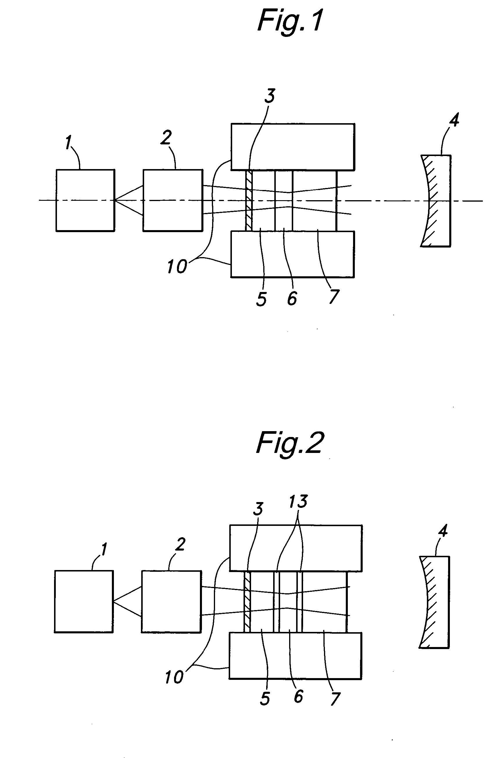
[0056] Referring to FIG. 2 showing the second embodiment of the present invention, the laser diode 1 serving as a pumping light source, pumping optical system 2 and output mirror 4 are similar to those of the first embodiment. The dimensions of the first laser crystal 5 are similar to those of the counterpart in the first embodiment. The dielectric multi-layer film 3 on the side of the pumping optical system 2 is similar to that of the first embodiment, but the opposite face of the first laser crystal 5 is coated with a dielectric layer having a low reflectivity for the Nd:YVO4 laser at 1,064 nm.

[0057] The second laser crystal 6 is similar to that of the first embodiment in terms of dimensions and Nd3+ concentration. However, the two ends surfaces through which the pumping light passes are each coated with a dielectric layer having a low reflectivity for both the Nd:YVO4 output laser at 1,064 nm and the pumping laser at 809 nm. The second laser crystal 6 is spaced from the first la...

third embodiment

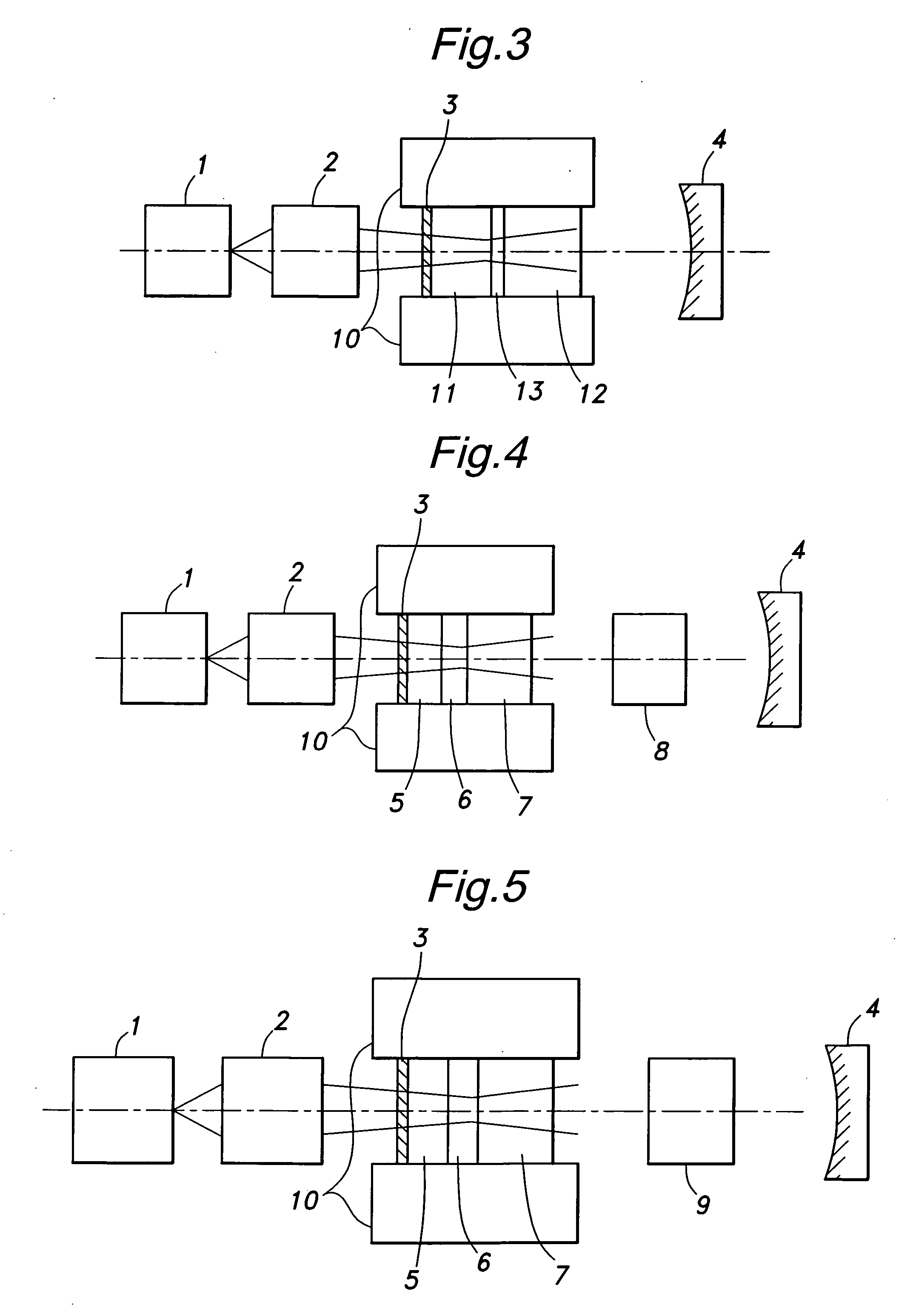
[0061] Referring to FIG. 3 showing the third embodiment of the present invention, the laser crystal in this case consisted of two individual laser crystals 11 and 12 made of Nd:YVO4 crystals. The face of the first laser crystal 11 closer to the pumping optical system 2 was provided with a dielectric multi-layer film mirror 3, and the second laser crystal 12 was spaced from the first laser crystal 11 by a gap 13.

[0062] The first laser crystal 11 had a Nd3+ concentration of 0.2 atomic %, and was 1.5 mm long. The face of the first laser crystal closer to the pumping optical system was provided with a dielectric multi-layer film mirror 3, and the opposite face was coated with a dielectric layer having a low reflectivity for both the Nd:YVO4 laser at 1,064 nm and pumping laser at 808 nm.

[0063] The second laser crystal 12 had a Nd3+ concentration of 1.1 atomic %, and was 3.5 mm long. The two opposite faces through which the pumping laser and output laser respectively pass through were e...


PUM


Abstract

In an end pumped or axially pumped solid state laser using a laser diode as a pumping light source, the laser crystal comprises a plurality of individual laser crystals arranged along an axial direction that have progressive higher concentrations of rare earth irons toward the output end. By thus arranging the individual laser crystals containing varying concentrations of rare earth ions, the absorption of laser for each length can be made uniform so that the tolerance for a high power pumping light is increased, and the laser output can be maximized without damaging the laser crystal.

Description

CROSS REFERENCE TO RELATED APPLICATIONS [0001] The present application claims priority from Japanese application No. 2003-323841, filed Sep. 17, 2003. TECHNICAL FIELD [0002] The present invention relates to end pumped or axially pumped solid state lasers using a semiconductor device such as a laser diode as a pumping light source, and in particular to such lasers capable of producing a large output without the risk of the intense pumping light damaging the laser crystal. BACKGROUND OF THE INVENTION [0003] Various forms of solid state lasers using a semiconductor light source and a laser crystal added with rare earth ions have been proposed. In particular, end pumped or axially pumped lasers of this type are particularly preferred because of the ease in achieving a mode matching between the pumping light and laser output. Therefore, a relatively high efficiency can be achieved in converting the pumping light into the output laser light as compared with the side pumped solid state las...

Claims


Application Information

Patent Timeline
Patent Type & Authority Applications(United States)
IPC IPC(8): H01S3/04H01S3/06H01S3/07H01S3/08H01S3/0941H01S3/14H01S3/16
CPCH01S3/0405H01S3/0604H01S3/0617H01S3/07H01S3/09415H01S3/1673H01S3/117H01S3/1611H01S3/1643H01S3/1653H01S3/1671H01S3/109
Inventor KADOYA, MINORU
Owner SHOWA OPTRONICS
Why Eureka
Try Eureka