Method and system for controlling the presence of fluorine in refractory metal layers

a technology of refractory metal and fluorine, which is applied in the direction of chemically reactive gas growth, crystal growth process, polycrystalline material growth, etc., can solve the problems of compromising the structural and operational integrity of the underlying portion of the integrated circuit being formed, the deposition rate is much lower than typical cvd techniques by at least one order of magnitude, and the resistance of contacts is reduced, and the amount of fluorine present in the resulting refractory metal layer is substantially reduced

Inactive Publication Date: 2005-03-17
APPLIED MATERIALS INC
View PDF99 Cites 25 Cited by
  • Summary
  • Abstract
  • Description
  • Claims
  • Application Information

AI Technical Summary

Benefits of technology

[0011] A method and system reduces the resistance of contacts of refractory metal layers by controlling the presence of fluorine contained therein. The present invention is based upon the discovery that when employing ALD techniques to form refractory metal layers on a substrate, the carrier gas employed impacts the presence of fluorine in the resulting layer. As a result, the method features chemisorbing onto the substrate alternating monolayers of a first compound and a second compound, with the second compound having fluorine atoms associated therewith, with each of the first and second compounds being introduced into the processing chamber along with a carrier gas; and controlling a quantity of the fluorine atoms associated with the monolayer of the second compound as a function of the carrier gas. Specifically, it was found that by introducing the first and second compounds employing H2 as a carrier gas, the amount of fluorine present in the resulting refractory metal layer was substantially reduced, compared to employing either nitrogen, N2, or argon, Ar, as a carrier gas.

Problems solved by technology

These requirements become more critical as substrate size increases, creating a need for more complexity in chamber design and gas flow technique to maintain adequate uniformity.
A drawback with ALD techniques is that the deposition rate is much lower than typical CVD techniques by at least one order of magnitude.
Employing the aforementioned deposition techniques it is seen that formation of a layer at a high deposition rate while providing adequate step coverage are conflicting characteristics often necessitating sacrificing one to obtain the other.
For example, blanket deposition of a tungsten layer on a semiconductor wafer is time-consuming at temperatures below 400° C. The deposition rate of tungsten may be improved by increasing the deposition temperature to, e.g., about 500° C. to about 550° C. Temperatures in this range may compromise the structural and operational integrity of the underlying portions of the integrated circuit being formed.
Finally, tungsten has proven difficult to deposit uniformly.
This has been shown by variance in tungsten layers' thickness of greater than 1%, which frustrates control of the resistivity of the layer.

Method used


Image

  • Method and system for controlling the presence of fluorine in refractory metal layers
  • Method and system for controlling the presence of fluorine in refractory metal layers
  • Method and system for controlling the presence of fluorine in refractory metal layers

Examples


Embodiment Construction

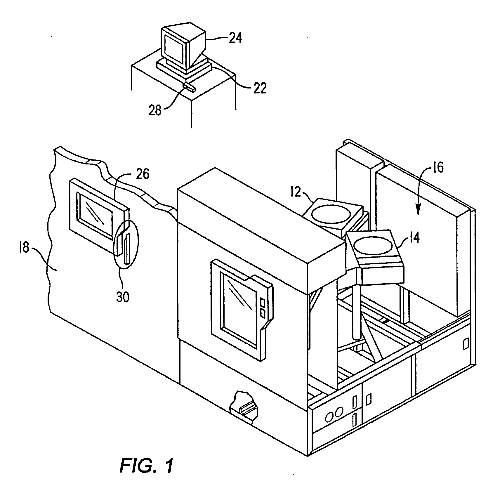
[0028] Referring to FIG. 1, an exemplary wafer processing system includes two or more processing chambers 12 and 14 disposed in a common work area 16 surrounded by a wall 18. The processing chambers 12 and 14 are in data communication with a controller 22 that is connected to one or more monitors, shown as 24 and 26. The monitors typically display common information concerning the process associated with the processing chambers 12 and 14. One of the monitors 26 is mounted to the wall 18, with the remaining monitor 24 being disposed in the work area 16. Operational control of the processing chambers 12 and 14 may be achieved use of a light pen, associated with one of the monitors 24 and 26, to communicate with the controller 22. For example, light pen 28 is associated with monitor 24 and facilitates communication with the controller 22 through monitor 24. Light pen 30 facilitates communication with the controller 22 through monitor 26.

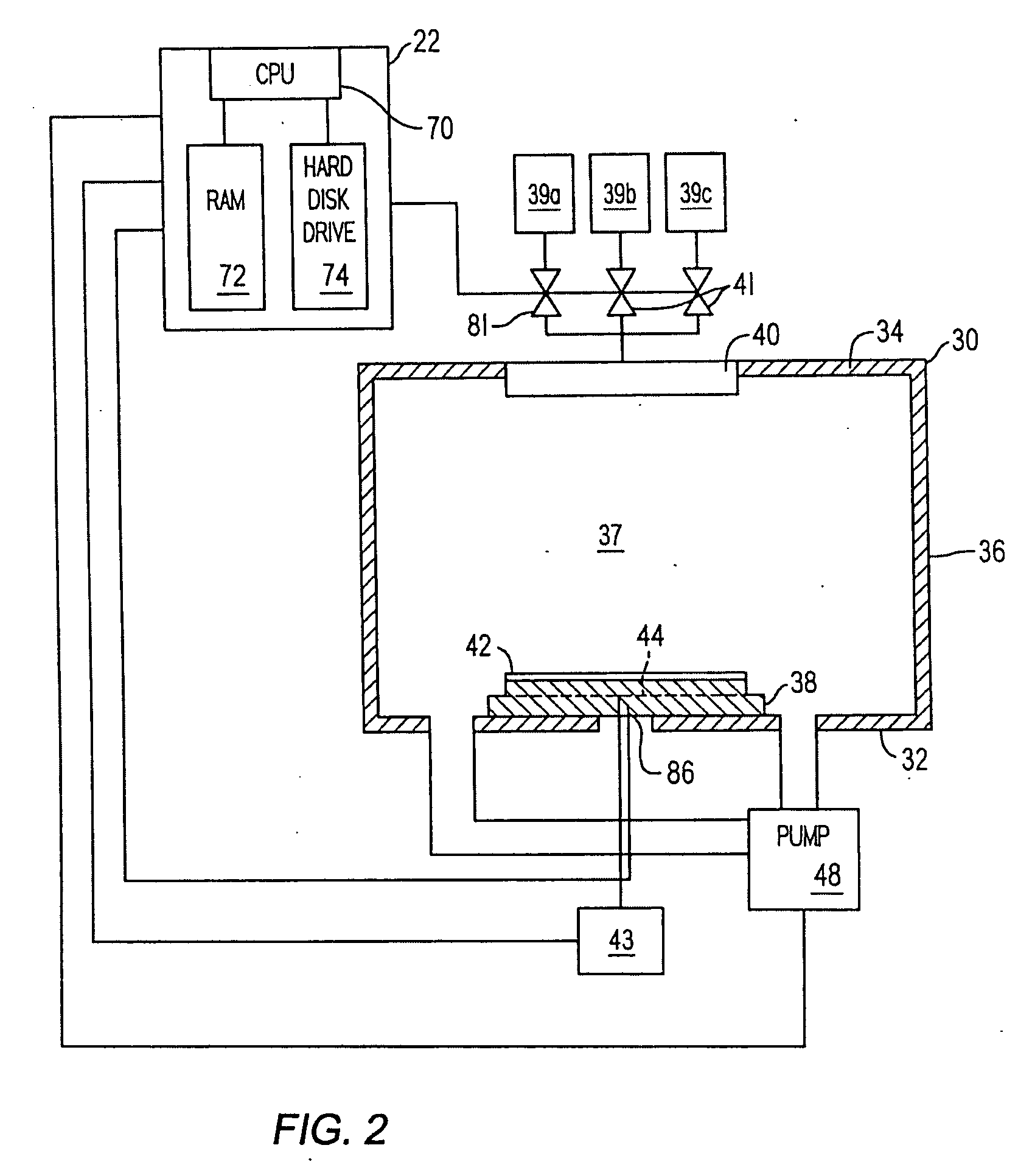
[0029] Referring both to FIGS. 1 and 2, each of ...


PUM

PropertyMeasurementUnit
Temperaturesaaaaaaaaaa
reflectivityaaaaaaaaaa

Abstract

A method and system to reduce the resistance of refractory metal layers by controlling the presence of fluorine contained therein. The present invention is based upon the discovery that when employing ALD techniques to form refractory metal layers on a substrate, the carrier gas employed impacts the presence of fluorine in the resulting layer. As a result, the method features chemisorbing, onto the substrate, alternating monolayers of a first compound and a second compound, with the second compound having fluorine atoms associated therewith, with each of the first and second compounds being introduced into the processing chamber along with a carrier gas to control a quantity of the fluorine atoms associated with the monolayer of the second compound.

Description

CROSS-REFERENCE TO RELATED APPLICATIONS [0001] This application is a continuation of co-pending U.S. patent application Ser. No. 09 / 625,336, filed Jul. 25, 2000, which is a divisional patent application of U.S. patent application Ser. No. 09 / 605,593, filed Jun. 28, 2000, now issued as U.S. Pat. No. 6,551,929.BACKGROUND OF THE INVENTION [0002] 1. Field of the Invention [0003] This invention relates to the processing of semiconductor substrates. More particularly, this invention relates to improvements in the process of depositing refractory metal layers on semiconductor substrates [0004] 2. Description of the Related Art [0005] The semiconductor processing industry continues to strive for larger production yields while increasing the uniformity of layers deposited on substrates having increasing larger surface areas. These same factors in combination with new materials also provide higher integration of circuits per unit area of the substrate. As circuit integration increases, the ne...

Claims


Application Information

Patent Timeline
Patent Type & Authority Applications(United States)
IPC IPC(8): C23C16/02C23C16/44C23C16/455C30B25/02C30B25/14H01L21/285H01L21/768
CPCC23C16/0272C23C16/14H01L21/76877C23C16/4401C23C16/45525C23C16/45527C23C16/45529C23C16/45534C23C16/45561C30B25/02C30B25/14H01L21/28556H01L21/28562H01L21/76838H01L21/76843H01L21/76876C30B29/38
Inventor KORI, MORISMAK, ALFRED W.BYUN, JEONG SOOLEI, LAWRENCE CHUNG-LAICHUNG, HUASINHA, ASHOKXI, MING
Owner APPLIED MATERIALS INC
Why Eureka
Try Eureka