Pattern forming apparatus

Inactive Publication Date: 2005-03-24
CANON KK
View PDF7 Cites 181 Cited by
  • Summary
  • Abstract
  • Description
  • Claims
  • Application Information

AI Technical Summary

Benefits of technology

[0017] The present invention is directed to a pattern forming apparatus cap

Problems solved by technology

However, on the other hand, there arise problems such that the cost for development and manufacturing of materials for lenses, which constitutes an optical system, and the cost required for equipment for replacing the optical path with inert gas are high.
However, according to this technology, a pattern is directly drawn on a wafer, and hence it takes an extremely long time for exposing a single piece of wafer.
Therefore, in the actual condition, it can only be applied to experimental manufacture or manufacture of device for specific use, which requires only a very small quantity, and he

Method used


Image

  • Pattern forming apparatus
  • Pattern forming apparatus
  • Pattern forming apparatus

Examples


first embodiment

[0039] [First Embodiment]

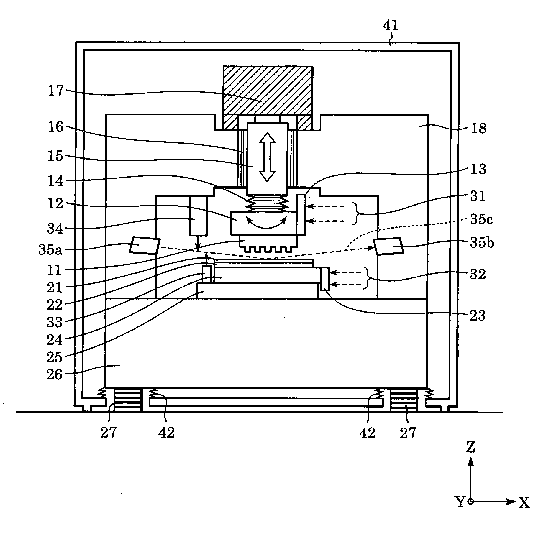
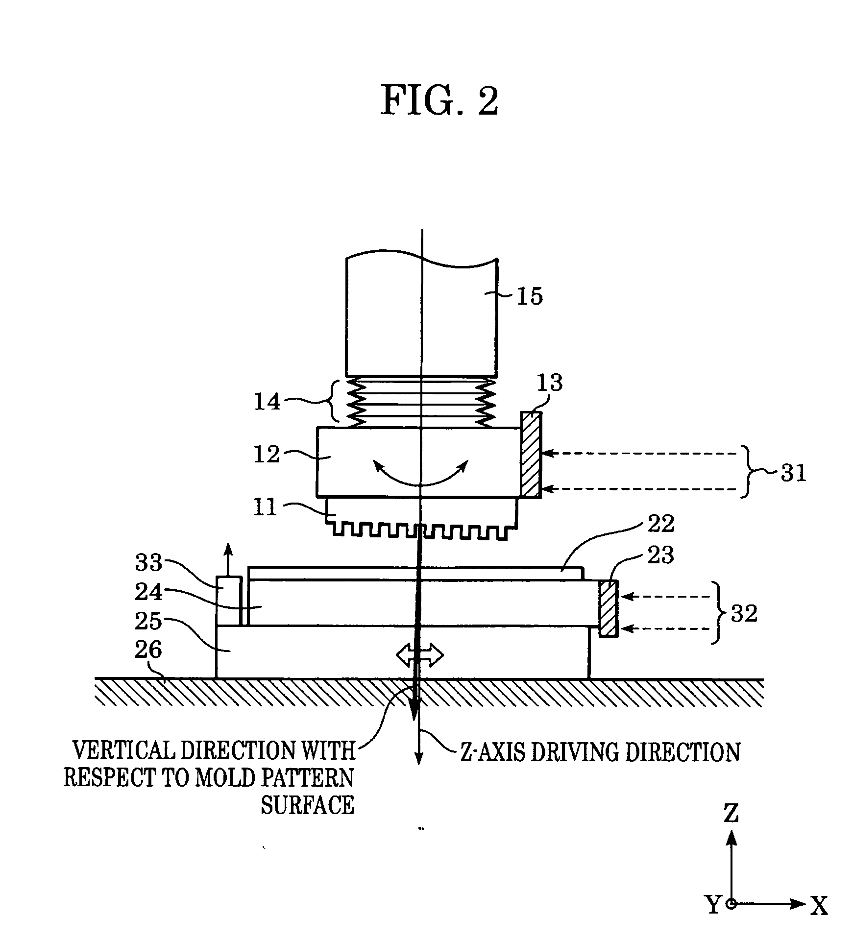
[0040]FIG. 1 is a drawing illustrating a pattern forming apparatus (nanoimprint apparatus) according to the present embodiment, showing a general structure of the apparatus. In order to facilitate the description, the directions are defined as shown by arrows in the drawing. The lateral direction is defined as X-axis, the perpendicular direction is defined as Y-axis, and the vertical direction is defined as Z-axis with respect to the plane of the drawing.

[0041] A mold 11 is an original plate and is formed with a fine pattern on the lower surface thereof by an Electron Beam Lithography or the like. The mold 11 is retained by a mold chuck 12 as a retaining device. The mold chuck 12 includes an electrostatic chuck for retaining an object with an electrostatic force and a mechanical chuck for retaining the object mechanically. A mold reference mirror 13 having extremely high level of flatness is fixed to the mold chuck 12, which serves as a measured section for...

second embodiment

[0070] [Second Embodiment]

[0071]FIG. 7 is a drawing illustrating the pattern forming apparatus (nanoimprint apparatus) according to the present embodiment, and showing a general structure of the entire apparatus. In order to facilitate the description, the directions are defined as shown by arrows in the drawing. The lateral direction is defined as X-axis, the perpendicular direction is defined as Y-axis, and the vertical direction is defined to Z-axis with respect to the plane of the drawing. The like reference member as in the first embodiment are represented by the same reference numerals.

[0072] The mold 11 is an original plate and is formed with a fine pattern on the lower surface thereof by an EB drawing apparatus or the like. The mold 11 is retained by a mold chuck 12 as a retaining device. The mold chuck 12 includes an electrostatic chuck for retaining an object with an electrostatic force and a mechanical chuck for retaining the object mechanically. A mold reference mirror ...

third embodiment

[0102] [Third Embodiment]

[0103] Subsequently, an embodiment of a manufacturing method of a device utilizing the above-described fine processing apparatus will be described.

[0104]FIG. 15 shows a manufacturing flow of a semiconductor device (semiconductor chip such as an IC or LSI, a liquid crystal panel, a CCD, etc . . . . ). In Step 1 (circuit design), a circuit of the semiconductor device is designed. In Step 2 (mold manufacturing), a mold on which the designed circuit pattern is formed is manufactured. On the other hand, in Step 3 (wafer manufacturing), a wafer is manufactured using material such as silicon. Step 4 (wafer process) is referred to as preprocess, where an actual circuit is formed on the wafer using the prepared mold and the wafer. The subsequent Step 5 (assembly) is referred to as post-process, which is a process for obtaining chips using the wafer manufactured in Step 5 and includes an assembling step (dicing, bonding), a packaging step (encapsulation of the chip)....


PUM


Abstract

A pattern forming apparatus maintaining alignment between a mold and a substrate. The pattern forming apparatus includes a press pressing the mold against the substrate in a pressing direction, and a mechanism to maintain orientation of the mold and the substrate perpendicular to the pressing direction.

Description

CROSS REFERENCE TO RELATED APPLICATIONS [0001] This application claims priority from Japanese Patent Application No. 2003-331938 filed Sep. 24, 2003, which is hereby incorporated by reference herein. BACKGROUND OF THE INVENTION [0002] 1. Field of the Invention [0003] The present invention generally relates to an apparatus for forming a desired pattern and, more specifically, to a pattern forming apparatus using a technology of forming a desired pattern by pressing a mold on which the desired pattern is formed in advance to resin material (generally referred to as nanoimprint technology). [0004] 2. Description of the Related Art [0005] In recent years, the width of pattern lines on integrated circuits has reduced in association with an increase in density and speed of semiconductor integrated circuits, and hence further enhancement of capabilities in a method of manufacturing a semiconductor is required. Therefore, a KrF laser (248 nm), an ArF laser (193 nm), and an F2 laser (157 nm)...

Claims


Application Information

Patent Timeline
IPC IPC(8): G03F7/20G03F1/00G03F7/00G03F9/00H01L21/00H01L21/027H01L21/3205H01L21/768
CPCB82Y10/00B82Y40/00H01L21/67092G03F9/00G03F7/0002Y10S977/887
Inventor KASUMI, KAZUYUKI
Owner CANON KK
Why Eureka
Try Eureka