Plasma surface modification and passivation of organo-silicate glass films for improved hardmask adhesion and optimal RIE processing

Inactive Publication Date: 2005-03-31
IBM CORP
View PDF4 Cites 39 Cited by
  • Summary
  • Abstract
  • Description
  • Claims
  • Application Information

AI Technical Summary

Benefits of technology

[0011] It is also an object of the present invention to provide a BEOL interconnect structure with robust adhesion between the OSG surface and a hardmask.
[0012] It is also an object of the present invention to provide a BEOL interconnect structure with improved adhesion between hardmask films while eliminating buried densified layers. As stated above, such densified layers often result in severe micromasking effects during the RIE patterning of the interconnect structure.
[0013] These and other objects are achieved in the present invention by providing a method for fabricating a unique structure using OSG (porous, non-porous or a combination of porous and non-porous) and appropria

Problems solved by technology

As stated above, such densified layers often result in severe microma

Method used


Image

  • Plasma surface modification and passivation of organo-silicate glass films for improved hardmask adhesion and optimal RIE processing
  • Plasma surface modification and passivation of organo-silicate glass films for improved hardmask adhesion and optimal RIE processing
  • Plasma surface modification and passivation of organo-silicate glass films for improved hardmask adhesion and optimal RIE processing

Examples


Embodiment Construction

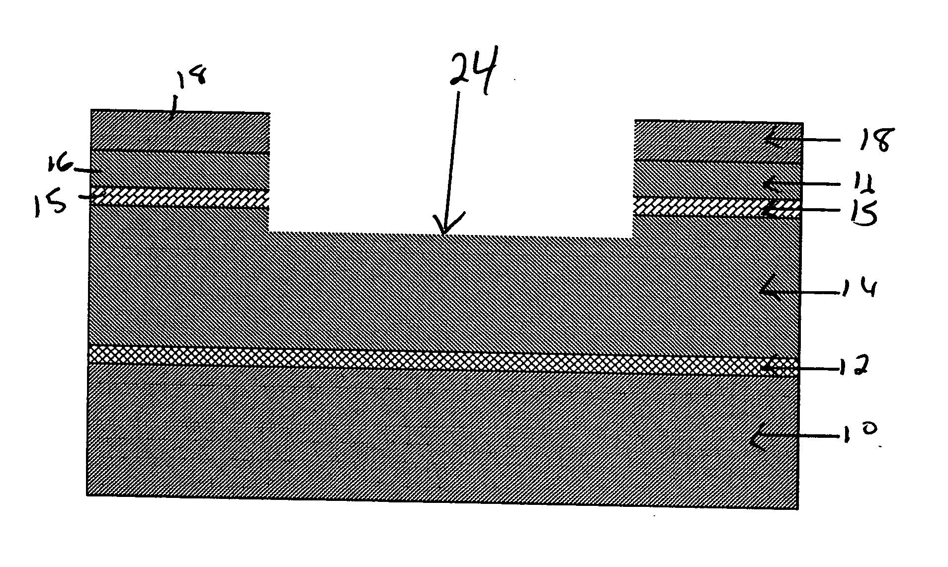
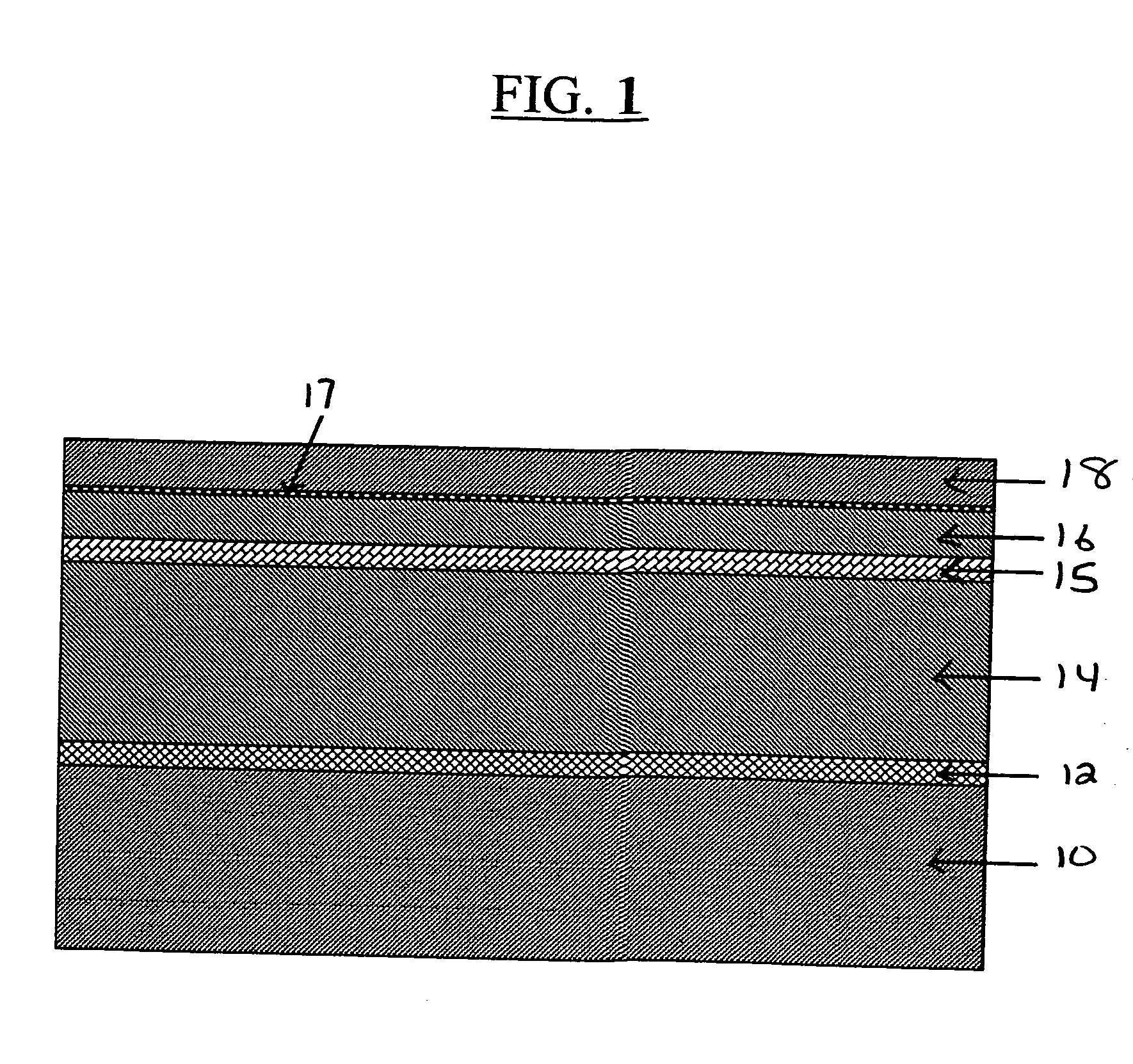
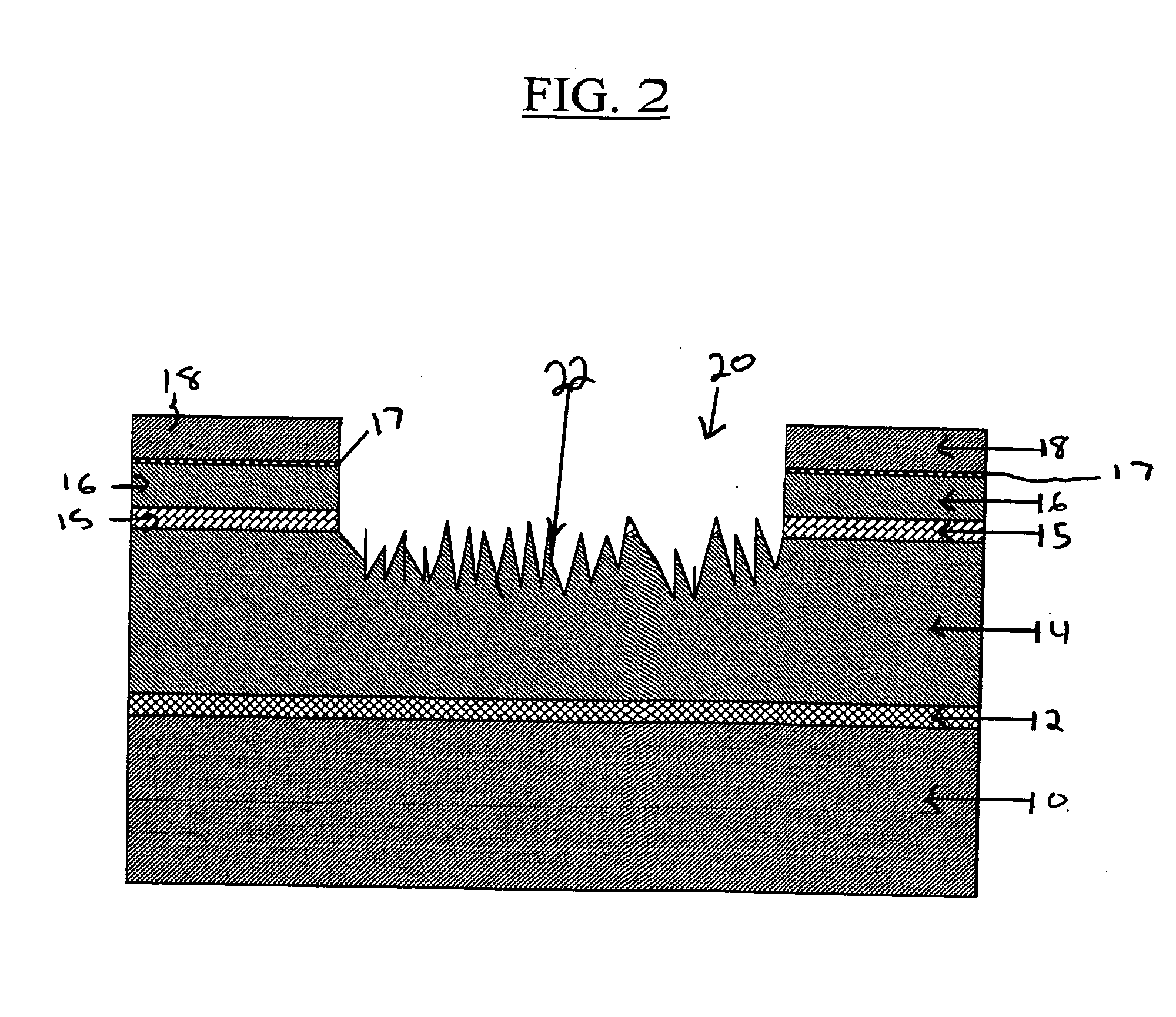
[0024] The present invention is directed to an interconnect structure useful for forming a semiconductor device, the interconnect structure having a low-k OSG dielectric layer, and an associated low-k hardmask dielectric stack. Enhanced adhesion between the OSG dielectric film and the hardmask dielectric stack is achieved by means of a mild plasma surface treatment of the OSG film surface. Typically, it has been observed and reported widely in the literature that plasma treatment of OSG films leads to an overall increase of the dielectric constant indicating damage to at least a surface layer of the OSG material. This damaged surface layer causes an increase in the capacitance and leakage within the dielectric material when subjected to an electrical stress, which leads to reliability failure of the interconnect structure.

[0025] The interconnect structure of the present invention is based on the surprising discovery that particular plasma conditions used to enhance the adhesion of ...


PUM


Abstract

Interconnect structure having enhanced adhesion between the various interfaces encompassing an organo-silicate glass (OSG) film, for use in semiconductor devices is provided herein. The novel interconnect structure includes a non-damaged plasma-treated low-k OSG surface to enhance the adhesion of the hardmask material to the OSG surface, and an unique deposition scheme for the hardmasks in order to make the entire structure pliant towards implementing mild processing condition during the reactive ion etch patterning of the dielectric structure in a damascene and dual-damascene scheme. The methods for making a semiconductor device having an enhanced adhesion and micromasks free profiles are also provided.

Description

FIELD OF THE INVENTION [0001] The present invention generally relates to integrated circuits (ICs), and more particularly to interconnect structures, including, for example, multilevel interconnect structures, in which the adhesion of a hardmask to an underlying dielectric film is significantly improved by employing a novel plasma treatment process. The present invention is also directed to a method of fabricating an interconnect structure using a hardmask stack that has significantly improved adhesion with the underlying dielectric film, while enabling gentler reactive ion etch (RIE) patterning conditions. BACKGROUND OF THE INVENTION [0002] Generally, semiconductor devices include a plurality of circuits which form an integrated circuit including chips (e.g., chip back end of line, or “BEOL”), thin film packages and printed circuit boards. Integrated circuits can be useful for computers and electronic equipment and can contain millions of transistors and other circuit elements that...

Claims


Application Information

Patent Timeline
IPC IPC(8): H01L21/033H01L21/312H01L21/768
CPCH01L21/02126H01L21/02203H01L21/02304H01L21/0234H01L21/76829H01L21/0332H01L21/3122H01L21/76802H01L21/76826H01L21/02362
Inventor AMERICA, WILLIAM G.DALTON, TIMOTHY J.KUMAR, KAUSHIK A.WICKLAND, HEIDI L.
Owner IBM CORP
Why Eureka
Try Eureka