Partially depleted SOI mosfet device

a soi mosfet, partially depleted technology, applied in the direction of semiconductor devices, electrical equipment, transistors, etc., can solve the problems of scaled bulk complementary metal-oxide-semiconductor (cmos) technology, power consumption, and insufficient power constraints of intended low-voltage applications, etc., to achieve relatively small chip surface area and high performance

Inactive Publication Date: 2005-04-07
UNITED MICROELECTRONICS CORP
View PDF16 Cites 18 Cited by
  • Summary
  • Abstract
  • Description
  • Claims
  • Application Information

AI Technical Summary

Benefits of technology

[0012] The primary object of the present invention is to provide a high performance partially depleted (PD) SOI MOSFET device, which consumes relatively small chip surface area.
[0013] Another object of the present invention is to provide a high performance partially depleted (PD) SOI MOSFET device with high current-driving capability and raised kink triggering voltage.
[0014] Still another object of at least one preferred embodiment of the present invention is to provide a process for fabricating the high performance PD SOI MOSFET device, which consumes relatively small chip surface area.

Problems solved by technology

The primary reason is the power consumption of scaled bulk complementary metal-oxide-semiconductor (CMOS) technology.
With the bulk CMOS 0.15 um technology, the effective channel length does not work satisfactorily within the power constraints of the intended low-voltage applications.
However, despite these advantages of the SOI technology, this technology faces some key challenges in process and manufacturing availability, devices and circuit design issues.
At device and circuit level, the floating body effect and the so-called kink effect in partially depleted devices poses major challenges for large-scale design.
One drawback of the above-mentioned prior art disclosures is that the manufacturing process for making an SOI MOSFET device having H-gate or T-gate body tie configurations is complicated.
Further, prior art body tied SOI device has poor device performance due to eliminated floating body effect.
In addition, such body-tied SOI devices according to the prior art usually need an additional body contact that consumes a lot of chip surface area.

Method used


Image

  • Partially depleted SOI mosfet device
  • Partially depleted SOI mosfet device
  • Partially depleted SOI mosfet device

Examples


Embodiment Construction

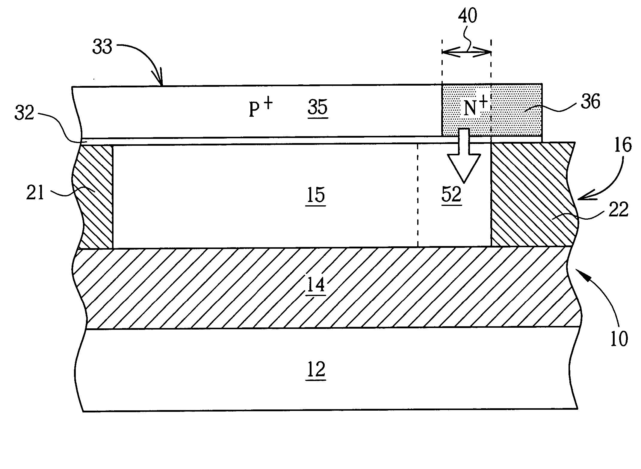
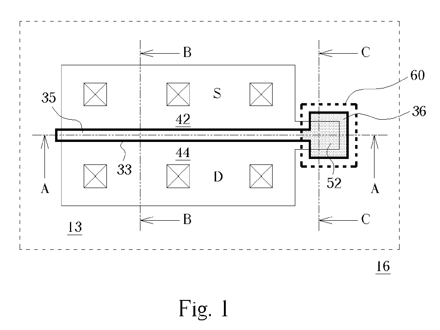
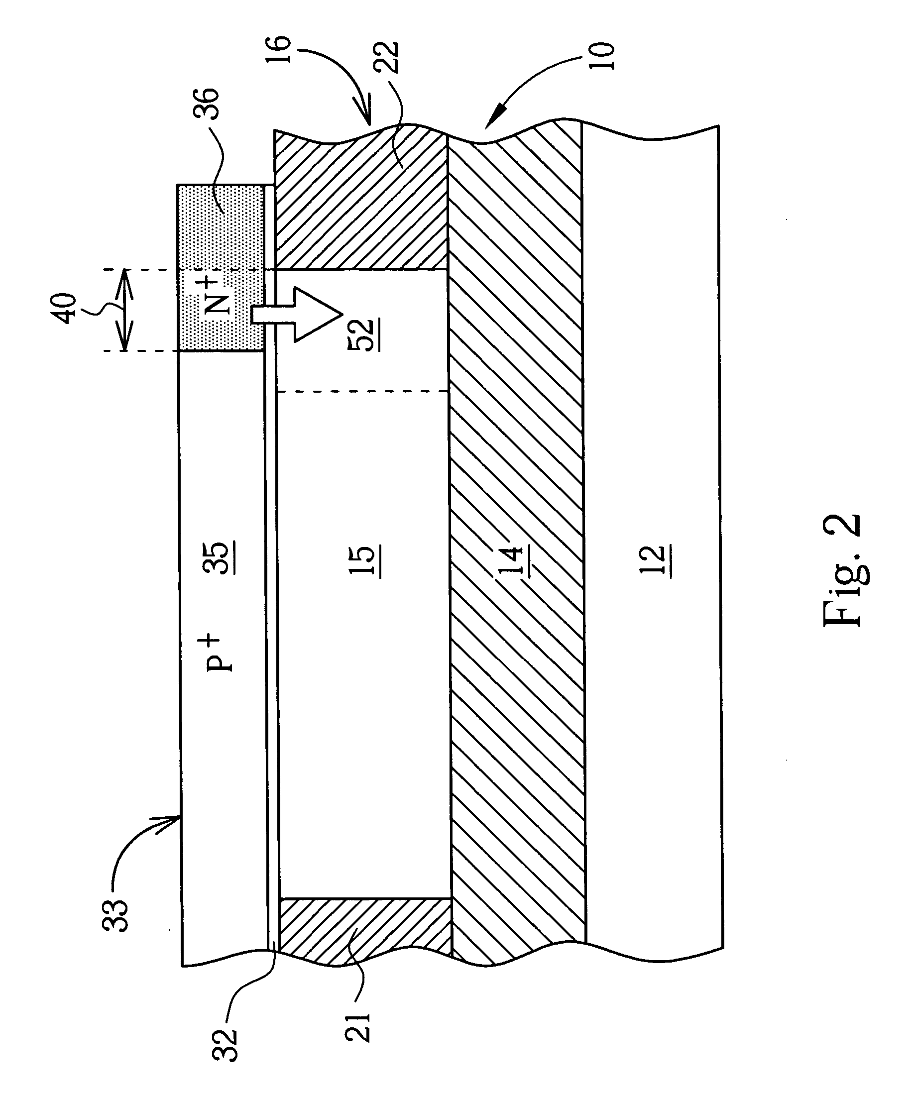
[0025] Please refer to FIG. 1 to FIG. 4, wherein FIG. 1 is a top view layout of one preferred embodiment of a PD SOI MOSFET in accordance with the present invention, FIG. 2, FIG. 3, and FIG. 4 are cross-sectional views taken from lines A-A, B-B, and C-C of FIG. 1, respectively. The first preferred embodiment of the present invention through FIGS. 1 to 4 demonstrates a PMOS SOI device. However, it is understood by those skilled in the art that the SOI integrated circuit of the present invention could be implemented using N-MOSFETs and P-MOSFETs by applying appropriate reversal of conductivity types. As shown in FIG. 1 and FIG. 2, a commercially available SOI substrate 10 is provided. The SOI substrate may be formed by any suitable method, such as the separation by implanted oxygen (SIMOX) method or the bonded-and-etch back (BESOI) method. By way of example, the SOI substrate 10 is a SIMOX wafer with a buried oxide insulation layer 14 supported by a support substrate 12. The thickness...


PUM


Abstract

A partially depleted SOI MOS device includes a well of first conductivity type isolated in a thin film body of an SOI substrate. The SOI substrate encompasses the thin film body, a support substrate, and a buried oxide layer interposed between the thin film body and the support substrate. A gate dielectric layer is disposed on a surface of the well. A polysilicon gate is patterned on the gate dielectric layer. The polysilicon gate consists of a first gate section of first conductivity type overlapping with an extended well region of the well and a second gate section of second conductivity type lying across the well, whereby a tunneling connection is formed between the first gate section and the extended well region of said well. Source and drain regions of second conductivity type are formed on opposite sides of the second gate section.

Description

BACKGROUND OF INVENTION [0001] 1. Field of the Invention [0002] The present invention relates in general to semiconductor devices, and in particularly, to high performance partially depleted (PD) SOI MOSFET devices. According to one preferred embodiment of the present invention, a PD SOI MOSFET device with high current-driving capability is provided. [0003] 2. Description of the Prior Art [0004] Silicon-on-insulator (SOI) technology has long been used in many special applications such as radiation-hardened or high-voltage integrated circuits. It is only in recent years that SOI has emerged as a serious contender for low-power high-performance applications. The primary reason is the power consumption of scaled bulk complementary metal-oxide-semiconductor (CMOS) technology. With the bulk CMOS 0.15 um technology, the effective channel length does not work satisfactorily within the power constraints of the intended low-voltage applications. Having the feature that the circuit elements a...

Claims


Application Information

Patent Timeline
Patent Type & Authority Applications(United States)
IPC IPC(8): H01L29/49H01L29/76H01L29/786
CPCH01L29/78615H01L29/4908
Inventor CHEN, SHIAO-SHIENHUANG, LU-SHIANGTANG, TIEN-HAO
Owner UNITED MICROELECTRONICS CORP
Why Eureka
Try Eureka