Scanning optical system

a scanning optical system and optical technology, applied in the field of optical microscopy, can solve the problems of optical resolution improvement that cannot be achieved by this method, imaging/probing system, restricted wavelength, etc., to prolong the useful life of traditional imaging components, improve imaging speed, and reduce cost

Active Publication Date: 2005-04-07
DCG SYST
View PDF10 Cites 20 Cited by
  • Summary
  • Abstract
  • Description
  • Claims
  • Application Information

AI Technical Summary

Benefits of technology

It is a further object of this invention to provide a hybridized method of combining traditional imaging with a low field of view lens, combined with imaging with a high NA, large field of view optical system in order to provide increased speed for the imaging operation;
It is a still furthe...

Problems solved by technology

Thus, whereas for lithography applications optical resolution can be improved by moving to shorter wavelengths, for many probing applications the wavelengths are restricted and the optical resolution improvement cannot be achieved by this method.
Prior methods for achieving high NA for imaging/probing systems have inherent drawbacks.
On...

Method used


Image

  • Scanning optical system
  • Scanning optical system
  • Scanning optical system

Examples


Embodiment Construction

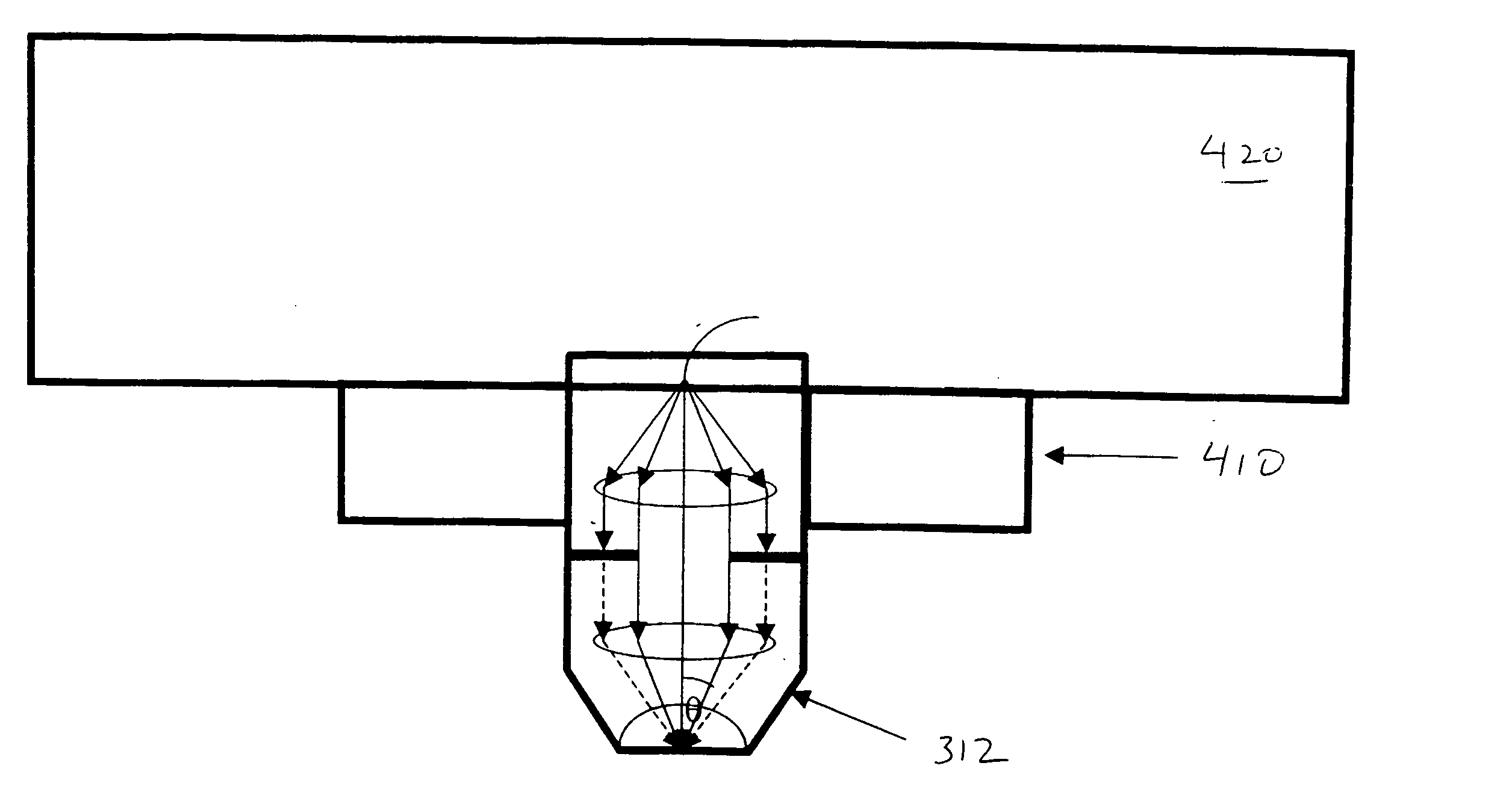
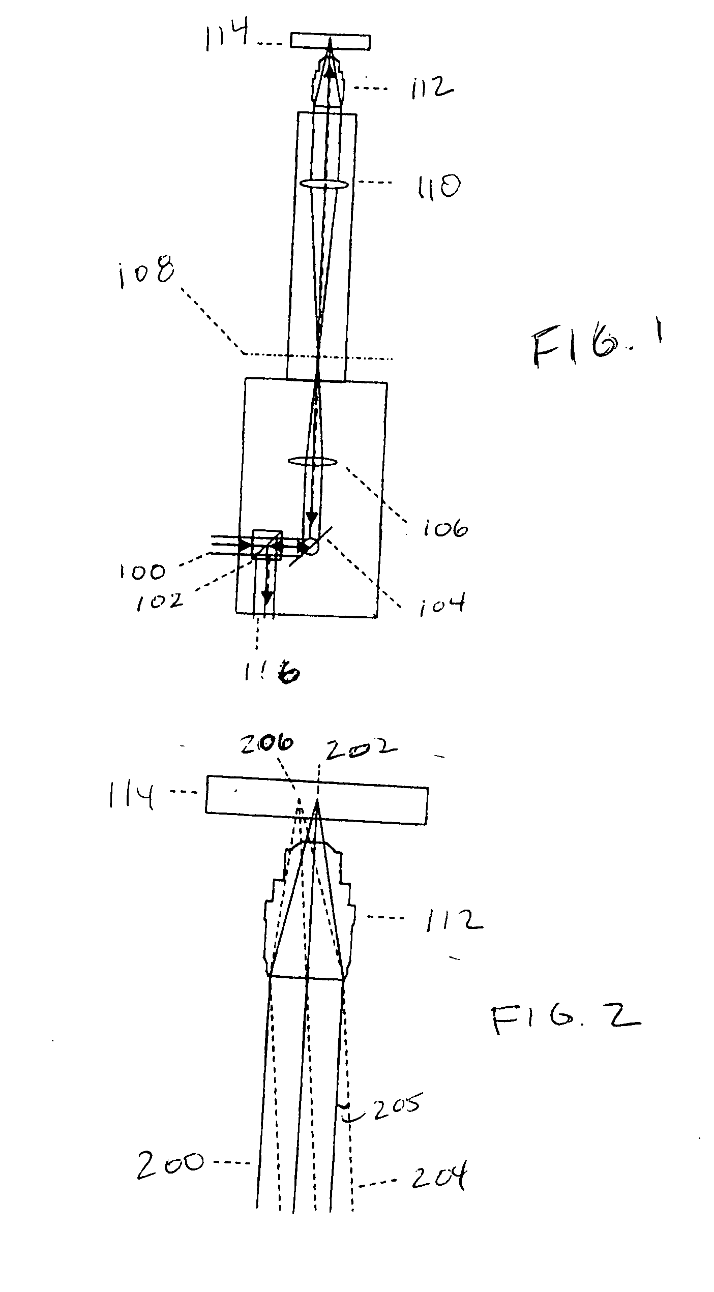
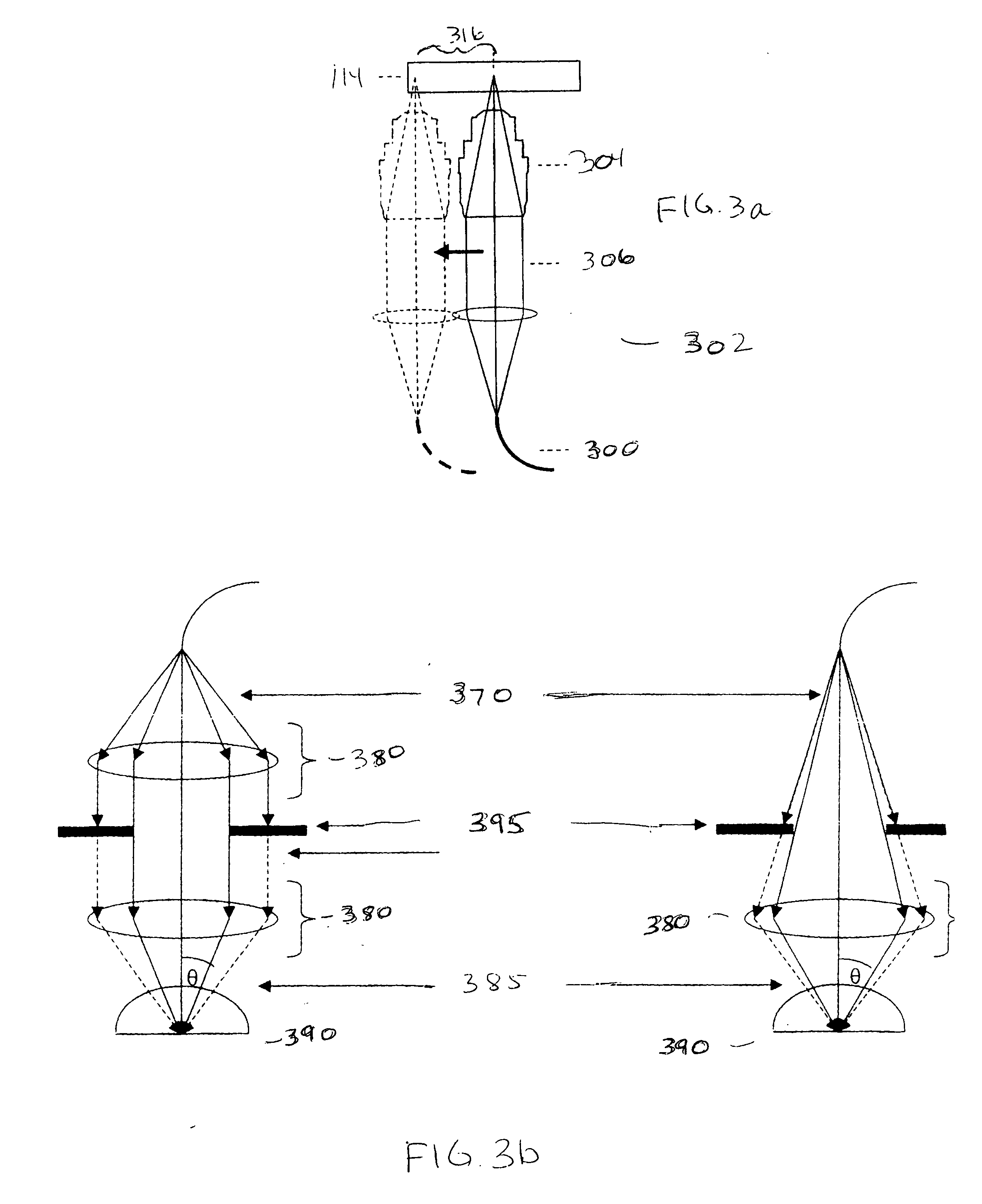
FIG. 1 illustrates the optical path of a conventional Laser Scanning Microscope (LSM), an example of which is the LSM-1064 manufactured by Checkpoint Technologies. Incident, collimated light 100 from a laser source (which may be delivered from a fiber+fiber collimator) impinges on beamsplitter 102, which is used to separate incident light from reflected light. Beamsplitter 102 may be a polarizing beamsplitter used in conjunction with a quarter-wave plate to improve transmission efficiency. Light 100 impinges on galvo-mirrors 104, which are rotated to generate a raster scan pattern of the light beam incident on a sample. Generally, two galvo-mirrors are used, one for x-scan and another for y-scan. There are alternative means for generating a raster scan pattern, such as acousto-optic crystals, or tip-tilt piezo scanners. These methods are described in Corle, T. R. and G. S. Kino, Confocal Scanning Optical Microscopy and Related Imaging Systems. 1996, San Diego: Academic Press, which ...


PUM


Abstract

A scanned optical system for use in optical probing applications provides a large Field of View (FOV) for objective lenses having high Numerical Aperture (NA), such as Solid Immersion Lenses (SIL's). This enables high resolution imaging of semiconductor devices for such applications as laser probing, TIVA/LIVA, OBIRCH, and photon emission timing analysis. A hybrid scanning optics configuration is disclosed to provide high resolution imaging over a small area along with low resolution imaging over a large area.

Description

FIELD OF THE INVENTION This invention relates to optical microscopy, and in particular to achieving increasingly high imaging resolution and high collection efficiency of an optical system used for integrated circuit probing. BACKGROUND OF THE INVENTION As integrated circuit geometries shrink, the resolution must be improved for optical systems which may be used in such applications as inspection systems and circuit probe and / or repair systems. Many probe systems used for complex circuitry having multiple metallization layers utilize backside probing and imaging. A description of a backside probing system including backside imaging is found in U.S. Pat. No. 6,518,571, issued Feb. 11, 2003. For backside imaging and probing through silicon, the transmission window of silicon combined with electro-optical effects in silicon restrict the useable optical wavelengths to the near infrared (NIR) region (900 nm to beyond 2000 nm). Thus, whereas for lithography applications optical resoluti...

Claims


Application Information

Patent Timeline
IPC IPC(8): G01N21/88G01N21/95G01N21/956
CPCG01N21/8806G01N21/9501G01N21/956G01N2201/103G01N2201/10G01N2201/101G01N2201/0853
Inventor LO, WILLIAM K.
Owner DCG SYST
Why Eureka
Try Eureka