

Gold alloy bonding wire for semiconductor device and process for producing the same
a technology of alloy bonding wire and semiconductor device, which is applied in the direction of yarn, solid-state devices, transportation and packaging, etc., can solve the problems of not being satisfied with the strength of the heat-affected portions, not being able to suppress the wire deformation or the strength of the wire, and not being able to improve the deformation of the wir
- Summary
- Abstract
- Description
- Claims
- Application Information
AI Technical Summary
Benefits of technology
Problems solved by technology
Method used
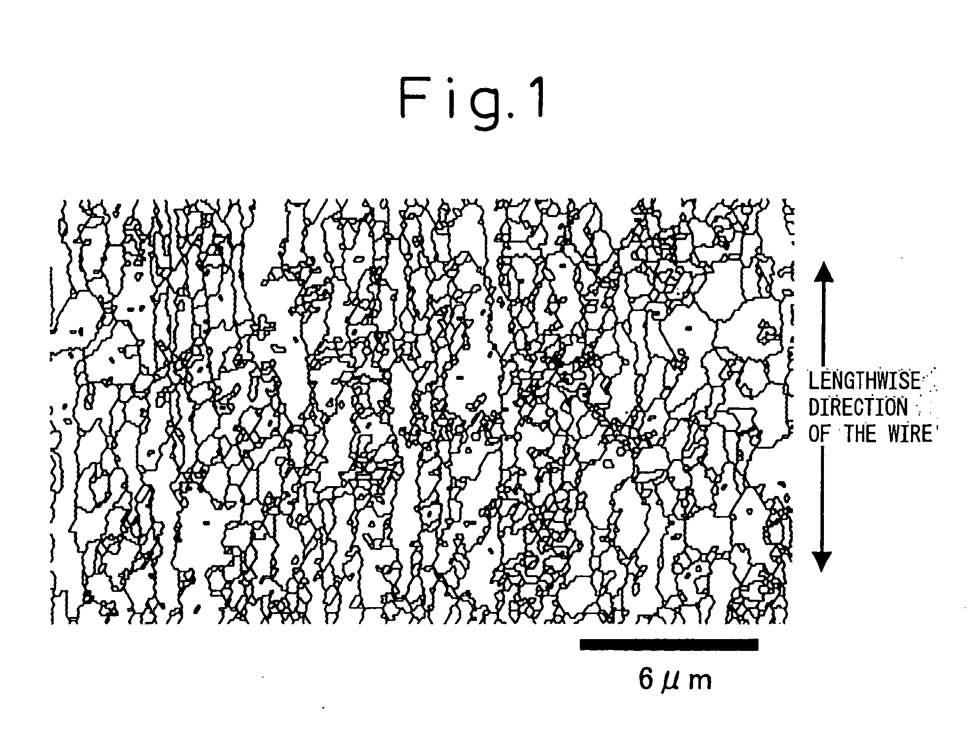
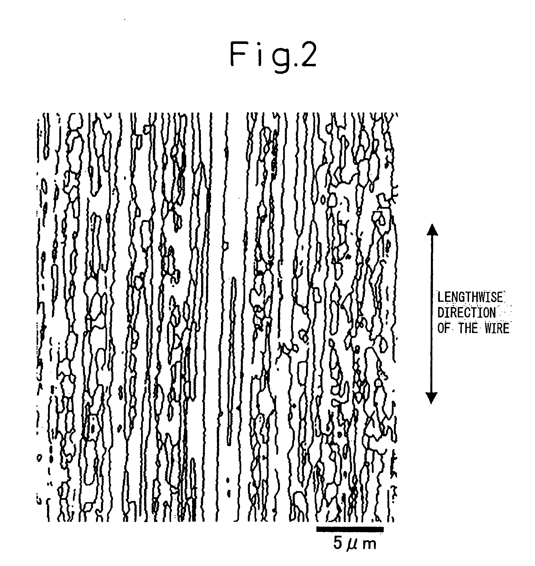
Image

Examples
example i
[0164] The bonding wires (1) to (14), (20) and (21) of the invention and the production methods (22) to (24) thereof will now be described by way of Examples.
[0165] By using electrolytic gold having a gold purity of not lower than about 99.995% by mass and by adding necessary components, the gold alloys having chemical components shown in Tables 1 to 5 were melted in a melting furnace and cast, the ingots thereof were rolled, pre-heat-treated in a heating furnace, drawn by using dies, and were after-heat-treated by continuously sweeping and heating the wires to thereby produce the bonding wires. The final wire diameter was selected to be, chiefly, not larger than 20 μm.
[0166] The steps of production will now be concretely described. First, an ingot of a diameter of 6 to 30 mm was prepared. In the step of rolling, the ingot was rolled by using a thin roll at a rate of 30 to 200 m / min until the wire diameter was 0.5 to 1.5 mm. In the step of pre-heat treatment, the wire was held in ...
example ii
[0208] The bonding wires (15) to (21) of the invention and the production methods (25) to (27) thereof will be described by way of Examples.
[0209] By using electrolytic gold having a gold purity of not lower than about 99.995% by mass, the gold alloys containing one or more kinds of elements selected from Be, Ca, La, In, Gd, Nd, Ce, Dy, Tb and Y at a total concentration in a range of 0.0005 to 0.02% by mass or containing one or more kinds of elements selected from Ag, Sn, Pb, Pt and Cu at a total concentration in a range of 0.003 to 0.1% by mass were melted in a melting furnace and cast, the ingots thereof were rolled, pre-heat-treated in a heating furnace, stretched by using dies, and were after-heat-treated by continuously sweeping and heating the wires to thereby produce the bonding wires. The final wire diameter was selected to be 20 μm.
[0210] Tables 8 and 9 illustrate area ratios of crystal orientations of the wires and use performance of the wire bonding.
[0211] Table 10 ill...
PUM
| Property | Measurement | Unit |
|---|---|---|
| temperature | aaaaa | aaaaa |
| diameter | aaaaa | aaaaa |
| temperature | aaaaa | aaaaa |
Abstract
Description
Claims
Application Information