Cold cathode electric field electron emission display device

a display device and electric field technology, applied in the field of cold cathode field emission display, can solve the problems of high brightness and size increase, damage to field emission device, and extremely impaired display quality, so as to improve the contrast of the display screen and prevent the collision of electrons

Inactive Publication Date: 2005-04-21
SONY CORP
View PDF2 Cites 34 Cited by
  • Summary
  • Abstract
  • Description
  • Claims
  • Application Information

AI Technical Summary

Benefits of technology

[0130] The phosphor material for constituting the phosphor layer can be selected from a fast-electron-excitation type phosphor material or a slow-electron-excitation type phosphor material. When the cold cathode field emission display is a monochrome display, it is not required to pattern the phosphor layer. When the cold cathode field emission display is a color display, preferably, the phosphor layers corresponding to three primary colors of red (R), green (G) and blue (B) patterned in the form of stripes or dots are alternately arranged. A black matrix may be filled in a gap between one patterned phosphor layer and another phosphor layer for improving the contrast of a display screen.
[0131] Further, the anode panel is preferably provided with a plurality of separation walls for preventing the occurrence of so-called optical crosstalk (color mixing) that is caused when electrons recoiling from the phosphor layer or secondary electrons emitted from the phosphor layer enter another phosphor layer, or for preventing the collision of electrons with other phosphor layer when electrons recoiling from the phosphor layer or secondary electrons emitted from the phosphor layer enter other phosphor layer over the separation wall.

Problems solved by technology

For applying the liquid crystal display to a floor-type television receiver, however, it still has problems to be solved concerning a higher brightness and an increase in size.
When the above abnormal discharge takes place, not only the display quality is extremely impaired, but also the anode electrode 34 and the field emission device are damaged.
Further, the potential in the cathode electrode 11 is increased, and as a result, the cathode-electrode control circuit 40 connected to the cathode electrode 11 may be damaged.
In a general production process of the cathode panels CP or the display panels using the cathode panels CP, practicing the above control involves great technical difficulties.

Method used


Image

  • Cold cathode electric field electron emission display device
  • Cold cathode electric field electron emission display device
  • Cold cathode electric field electron emission display device

Examples


example 1

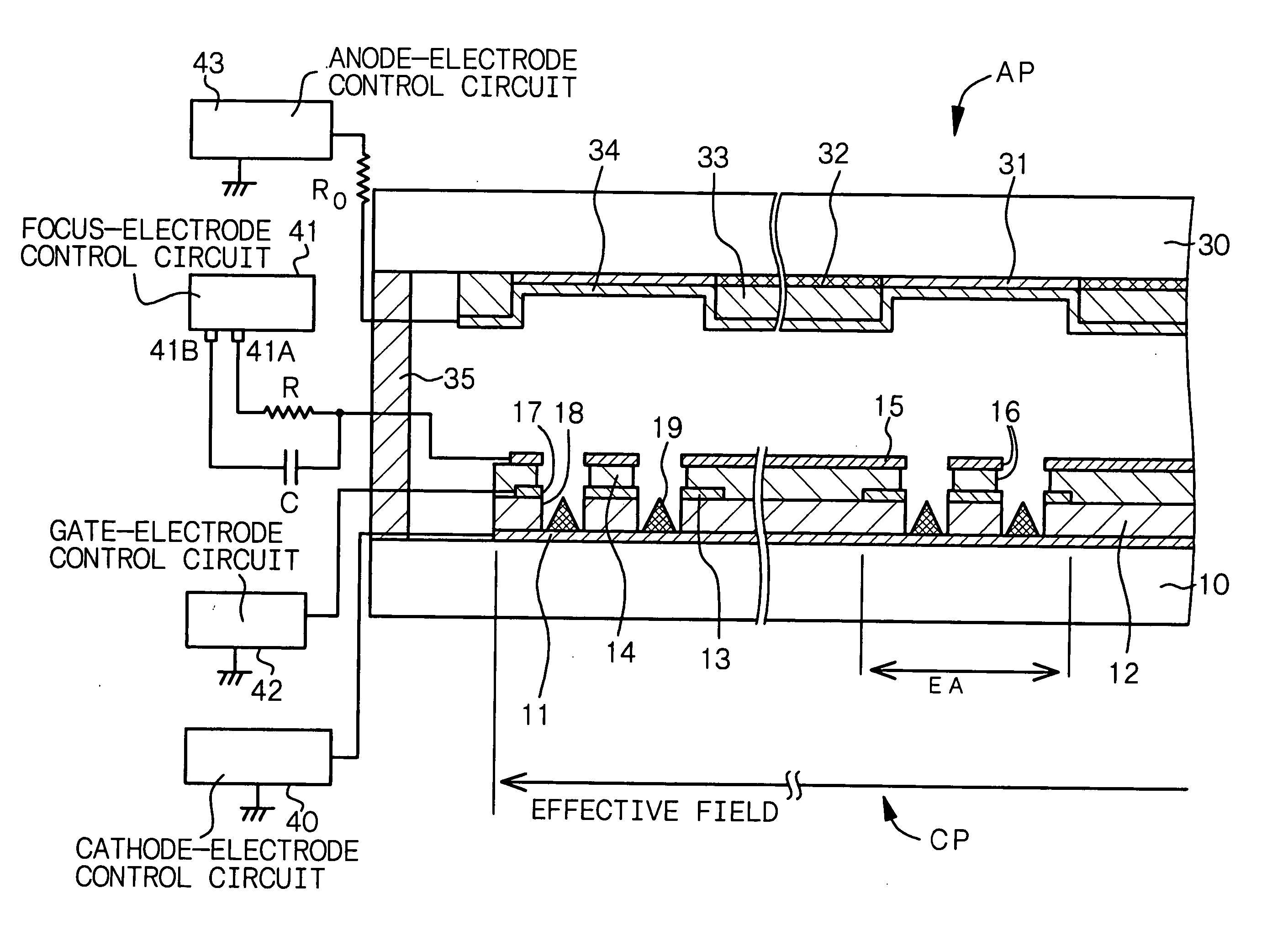
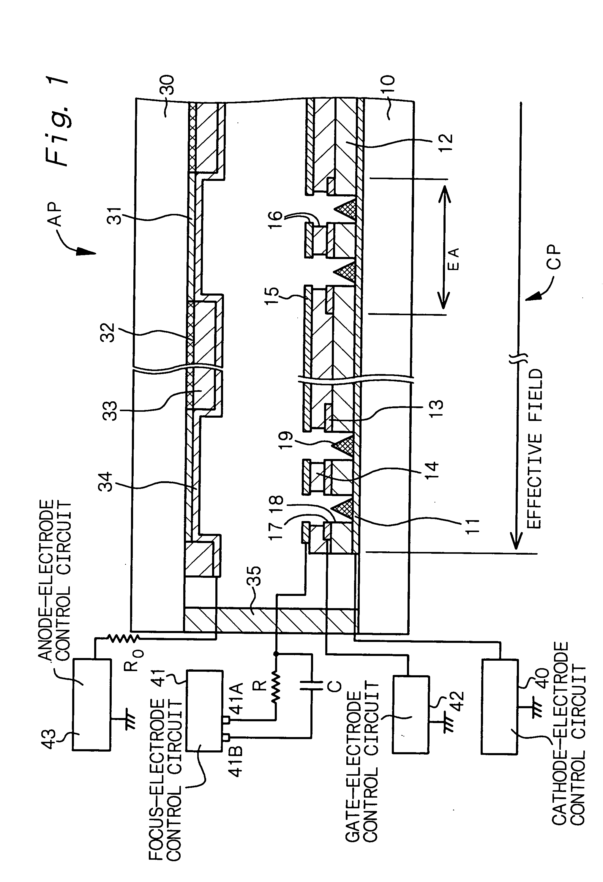
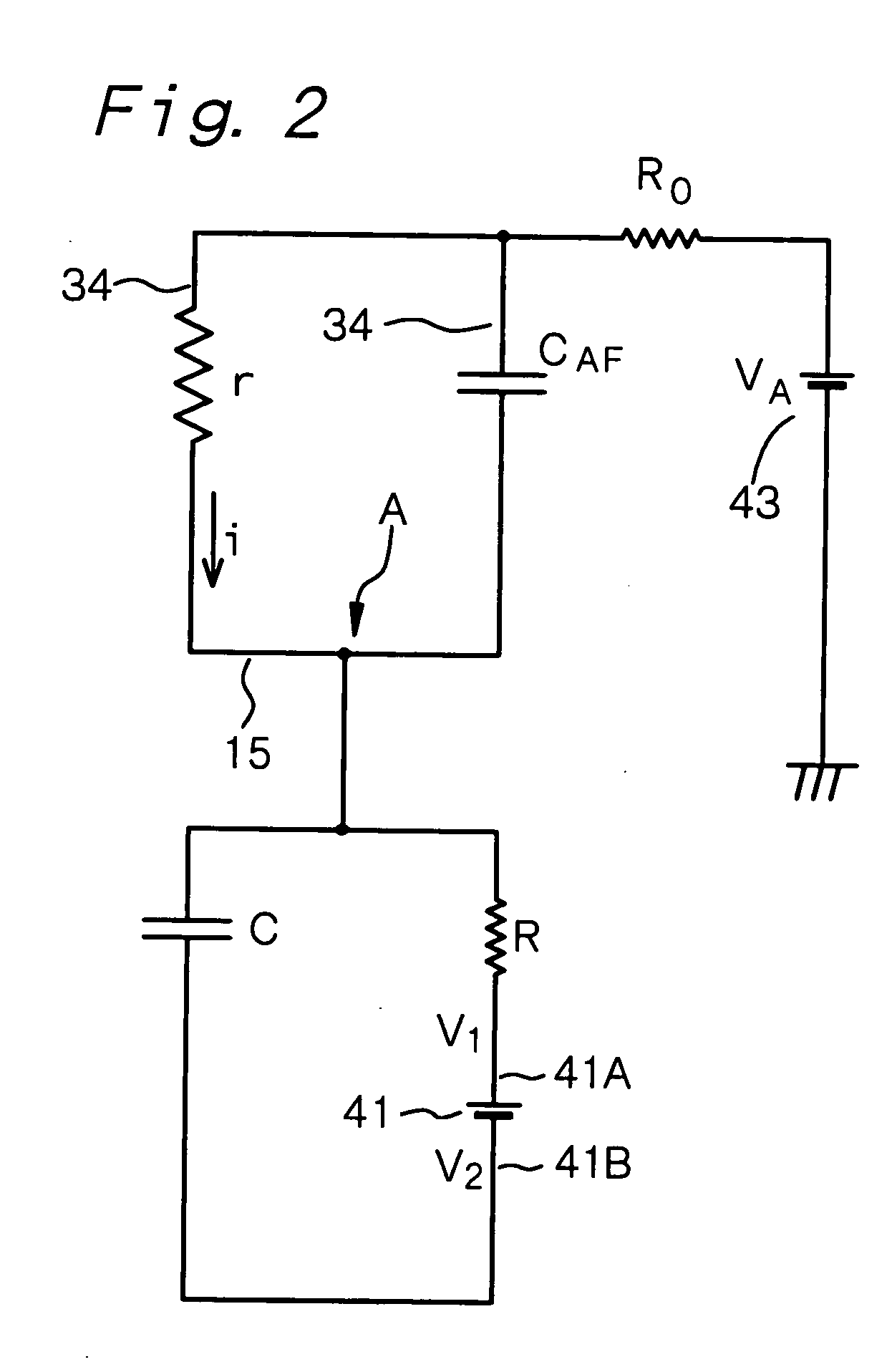
[0172] Example 1 is concerned with the cold cathode field emission display (to be abbreviated as “display” hereinafter) according to the first-A aspect of the present invention. FIG. 1 shows a schematic partial end view of a display panel for constituting a display having field emission devices, FIG. 13B shows a schematic partial end view of the field emission device, and FIG. 14 shows a schematic drawing of an electron-emitting region viewed from above. While many field emission devices are provided in an overlap region of a cathode electrode and a gate electrode, FIG. 13B shows one field emission device. When a cathode panel CP and an anode panel AP are exploded, the cathode panel CP has a schematic partial perspective view (however, an illustration of an insulating film and a focus electrode is omitted) as shown in FIG. 29.

[0173] The above display comprises at least; [0174] (A) a display panel in which a cathode panel CP having a plurality of electron-emitting regions EA and an ...

example 2

[0223] Example 2 is a variant of Example 1. Example 1 used the Spindt-type as a field emission device. In Example 2, the field emission device is a plane-type (a field emission device in which an electron-emitting portion having the form of a nearly flat plane is formed on the cathode electrode positioned in the bottom portion of the third opening portion).

[0224] An electron-emitting portion 19A constituting the plane-type field emission device in Example 2 comprises a matrix 52 and a carbon-nanotube structure (specifically, a carbon-nanotube 53) embedded in the matrix 52 in a state where the top portion of the carbon-nanotube structure is projected, and the matrix 52 is formed from an electrically conductive metal oxide (specifically, oxide-tin oxide, ITO) as shown in a schematic partial end view of FIG. 18B.

[0225] The production method of the field emission device will be explained with reference to FIGS. 17A, 17B, 18A and 18B, hereinafter.

[Step-200]

[0226] First, a stripe-shap...


PUM


Abstract

A cold cathode field emission display comprising at least (A) a display panel having a cathode panel CP provided with a plurality of electron-emitting regions EA and an anode panel AP provided with a phosphor layer 31 and an anode electrode 34, said cathode panel and said anode panel being bonded to each other in their circumferential regions, (B) a focus-electrode control circuit 41, (C) a resistance element R, and (D) a capacitor C, in which the focus electrode 15 formed in the electron-emitting region EA is connected to a first voltage-output portion 41A of the focus-electrode control circuit 41 through the resistance element R, and the focus electrode 15 is further connected to a second voltage-output portion 41B of the focus-electrode control circuit 41 through the capacitor C.

Description

TECHNICAL FIELD [0001] The present invention relates to a cold cathode field emission display and, more specifically, to a cold cathode field emission display with a focus electrode in which an increase in potential in the focus electrode can be suppressed even if an abnormal discharge takes place. BACKGROUND ART [0002] In the fields of displays for use in television receivers and information terminals, studies have been made for replacing conventionally mainstream cathode ray tubes (CRT) with flat-panel displays that are to comply with demands for a decrease in thickness, a decrease in weight, a larger screen and a high fineness. Such flat panel displays include a liquid crystal display (LCD), an electroluminescence display (ELD), a plasma display panel (PDP) and a cold cathode field emission display (FED). Of these, a liquid crystal display is widely used as a display for an information terminal. For applying the liquid crystal display to a floor-type television receiver, however,...

Claims


Application Information

Patent Timeline
Patent Type & Authority Applications(United States)
IPC IPC(8): H01J29/04G09G3/22H01J3/02H01J9/02H01J29/46H01J29/62H01J29/96H01J31/12
CPCG09G3/22G09G2320/0209G09G2320/046H01J9/025H01J29/467H01J2329/96H01J29/96H01J2329/08H01J2329/4604H01J2329/4695H01J29/481
Inventor KONISHI, MORIKAZU
Owner SONY CORP
Why Eureka
Try Eureka