Plasma processing method, plasma etching method and manufacturing method of solid-state image sensor

Inactive Publication Date: 2005-04-21
SANYO ELECTRIC CO LTD +1
View PDF9 Cites 21 Cited by
  • Summary
  • Abstract
  • Description
  • Claims
  • Application Information

AI Technical Summary

Problems solved by technology

An effect of the dark current is a noise in a signal appeared on

Method used


Image

  • Plasma processing method, plasma etching method and manufacturing method of solid-state image sensor
  • Plasma processing method, plasma etching method and manufacturing method of solid-state image sensor
  • Plasma processing method, plasma etching method and manufacturing method of solid-state image sensor

Examples


Embodiment Construction

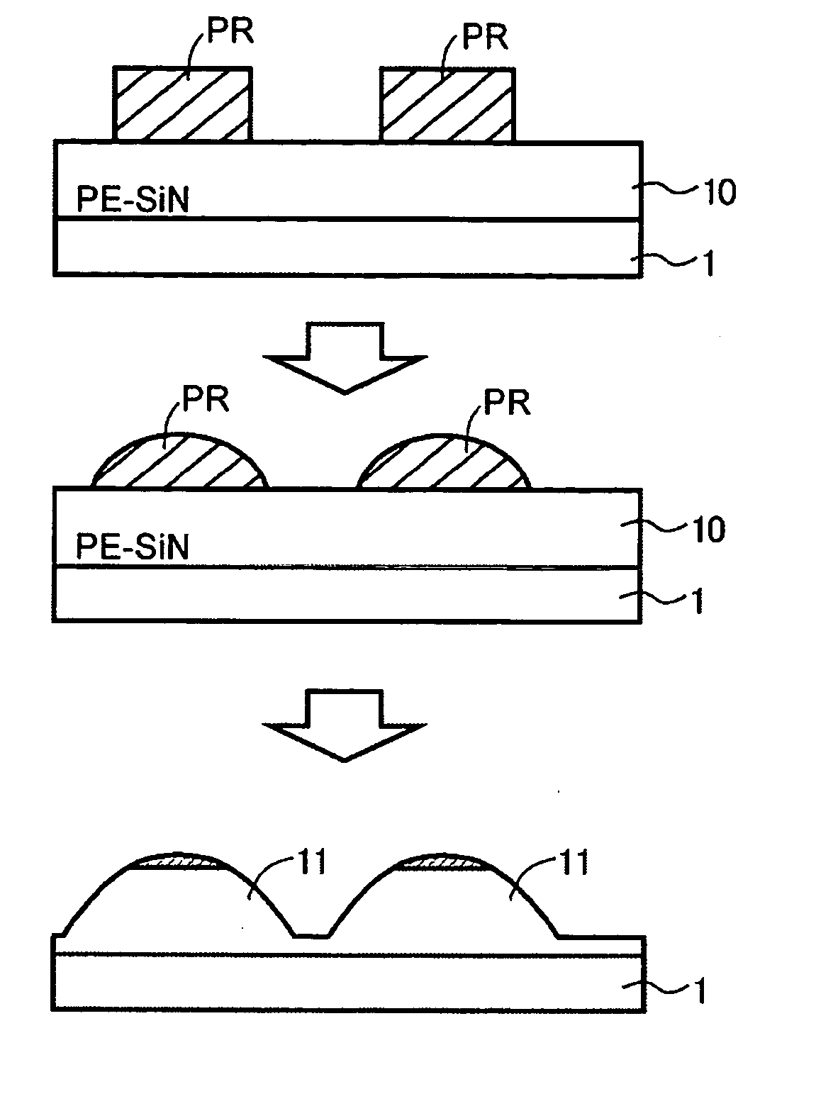
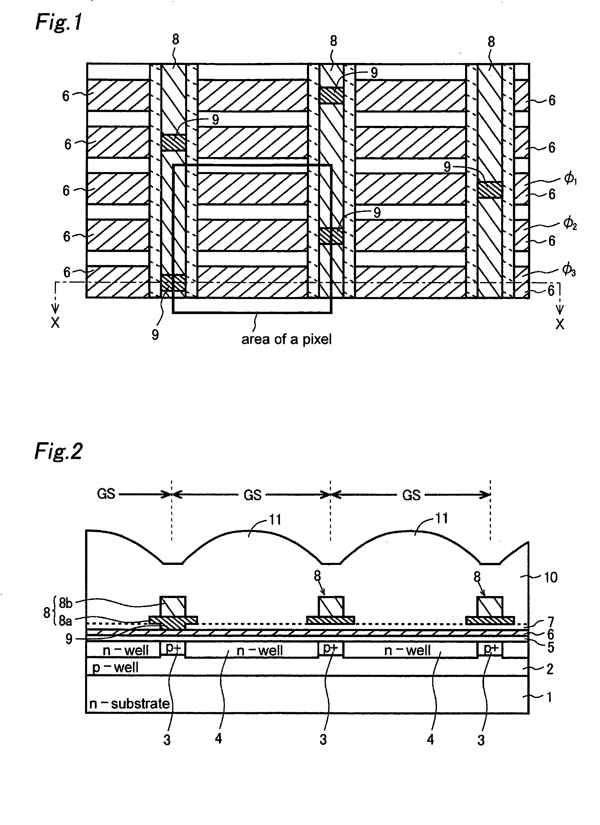
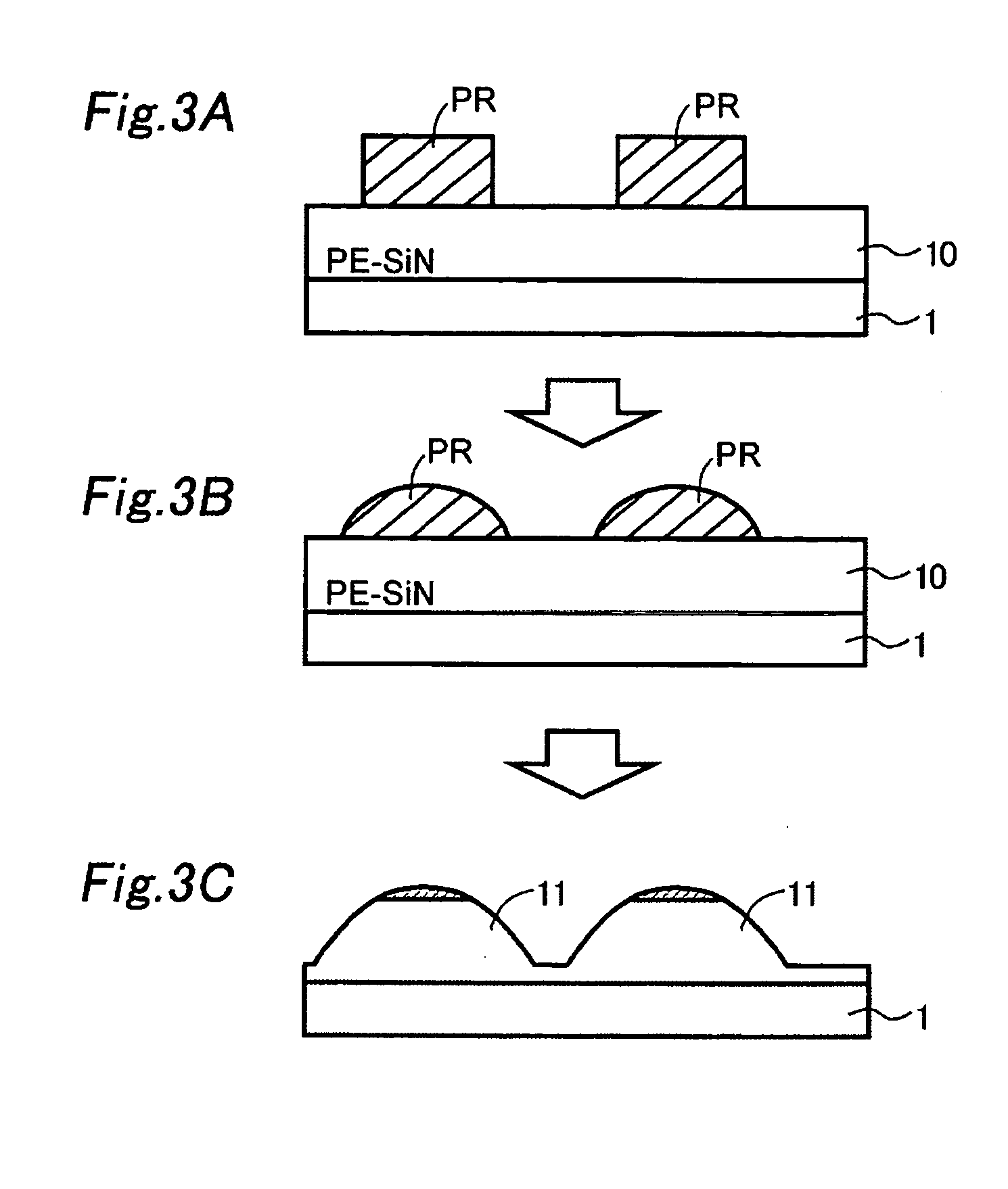
[0024] Next, an embodiment of this invention will be described referring to figures hereinafter. First, a structure of an image pick up portion of a CCD of this embodiment is applied will be explained referring to FIG. 1 and FIG. 2. FIG. 1 is a plan view showing the image pick up portion of the frame transfer type CCD and FIG. 2 is a cross-sectional view showing section X-X in FIG. 1.

[0025] A p-type well 2 is formed in a surface of an n-type silicon substrate 1. P+-type isolation regions 3 doped with high concentration of p-type impurities are formed in a surface of the p-type well 2 being separated from each other. An n-type well 4 is formed in each of spacing between the p+-type isolation regions 3. The n-type well 4 makes a channel region which serves as a transfer path for electric charges of information.

[0026] Each of a plurality of transfer gate electrodes 6 made of phosphor-doped polysilicon is formed on each of a plurality of the n-type wells 4 through a gate insulation fi...


PUM


Abstract

A method of plasma processing is offered to suppress generation of interface states, specifically to suppress increase in the dark current of a solid-state image sensor by reducing the interface states. An interlayer insulation film made of silicon nitride film is formed over a silicon substrate by plasma CVD, and a photoresist layer is selectively formed on the interlayer insulation film. Subsequent heating process makes a profile of the photoresist layer round. Next, the interlayer insulation film is plasma-etched using the photoresist layer as a mask and a fluorocarbon gas as an etching gas to form micro lenses. Pulse-time-modulated plasma method in which RF power is supplied intermittently is used to suppress increase in the interface states at silicon-silicon dioxide interface due to an influence of UV light generated in the plasma etching.

Description

CROSS-REFERENCE OF THE INVENTION [0001] This invention is based on Japanese Patent Application No. 2003-300256, the content of which is incorporated herein by reference in its entirety. BACKGROUND OF THE INVENTION [0002] 1. Field of the Invention [0003] This invention relates to a method of plasma processing, a method of plasma etching and a method of manufacturing solid-state image sensors using plasma etching, specifically to a technology to reduce interface states induced by plasma processing. [0004] 2. Description of the Related Art [0005] Solid-state image sensors such as CCDs (Charge Coupled Devices) and MOS image sensors are used in digital cameras and other video equipment in recent years. In a manufacturing process of the solid-state image sensors, the plasma processing is used in etching an insulation film formed on a silicon substrate and in depositing various kinds of films. [0006] Plasma used in the plasma processing is accompanied with generation of UV (ultraviolet) li...

Claims


Application Information

Patent Timeline
IPC IPC(8): H01L27/14H01L21/00H01L21/302H01L21/3065H01L21/311H01L21/461H01L21/84H01L27/148H05H1/00
CPCH01J37/32935H01L21/31116H01L27/14806H01L27/14685H01L27/14625H01L21/3065
Inventor OKIGAWA, MITSURUSAMUKAWA, SEIJI
Owner SANYO ELECTRIC CO LTD
Why Eureka
Try Eureka