Cavity-down semiconductor package with heat spreader

a technology of cavity-down semiconductor and heat spreader, which is applied in the direction of semiconductor devices, semiconductor/solid-state device details, electrical apparatus, etc., can solve the problems of serious damage to the reliability of the package and heat accumulation inside the substrate, and achieve the effects of improving substrate heat dissipation and substrate grounding capabilities, simplifying traditional grounding structures, and enhancing substrate adhesion

Inactive Publication Date: 2005-04-28
ADVANCED SEMICON ENG INC
View PDF7 Cites 11 Cited by
  • Summary
  • Abstract
  • Description
  • Claims
  • Application Information

AI Technical Summary

Benefits of technology

[0004] It is a primary object of the present invention to provide a cavity-down semiconductor package, including a heat spreader, a substrate with opening and a chip in the opening. A metal cover layer is formed over the inner surface of the substrate for attaching to the heat spreader. The metal cover layer is bonded to the heat spreader to establish a thermal-coupling relationship so as to replace the inner solder mask on the substrate and the ground layer inside the substrate to enhance substrate adhesion and improve substrate heat dissipation and substrate grounding capabilities.
[0005] It is a secondary object of the present invention to provide a cavity-down semiconductor package, which utilizes electrical vias of the substrate to electrically connect the metal cover layer on the substrate. The metal cover layer is formed over the inner surface of the substrate to attach to the heat spreader to simplify the traditional grounding structure.
[0006] It is a third object of the present invention to provide a chip carrier for cavity-down semiconductor package, which includes a heat spreader and an opening substrate with a metal cover layer. The metal cover layer, which may be formed by electroplating, sputtering or lamination, is formed over the inner surface of the substrate to attach to the heat spreader and to serve as an exposed ground layer of the substrate for replacing the solder mask on the inner surface of a substrate and the traditional ground layer inside a substrate to improve heat dissipation, electrical connection and grounding efficiencies between the substrate and the heat spreader.

Problems solved by technology

Because of the poor adhesion between the inner solder mask and the heat spreader and the poor moisture resistance of the adhesive resin, the substrate is easily separated from the heat spreader to cause delamination.
The reliability of the package is seriously affected.
That will lead to heat accumulation inside the substrate.

Method used


Image

  • Cavity-down semiconductor package with heat spreader
  • Cavity-down semiconductor package with heat spreader
  • Cavity-down semiconductor package with heat spreader

Examples


Embodiment Construction

[0010] Referring to the drawings attached, the present invention is described by means of the embodiment(s) below.

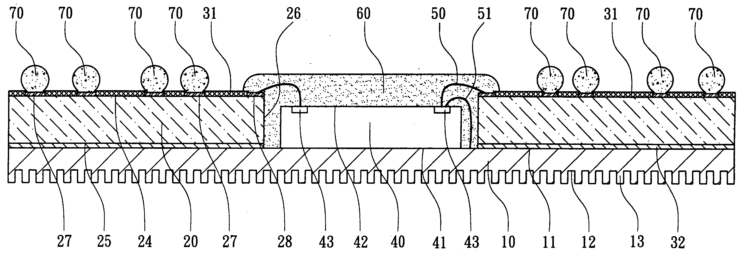
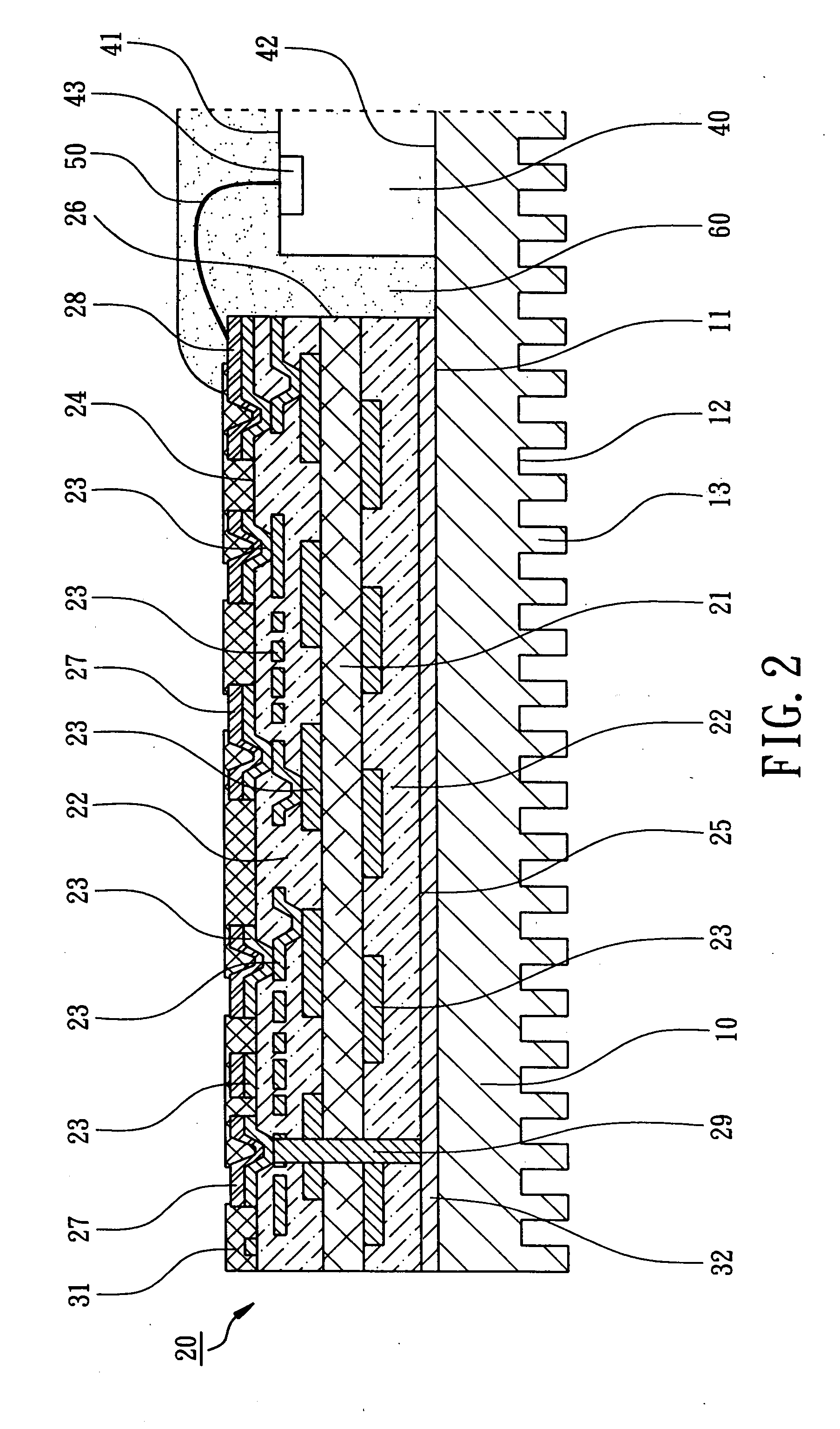
[0011] Referring to FIGS. 1 and 2, a cavity-down semiconductor package according to the embodiment of the present invention mainly comprises a heat spreader 10, a substrate 20, a chip 40 and an encapsulant 60. The heat spreader 10 is made of metal with excellent heat conduction and has a first surface 11 and a second surface 12. The first surface 11 of the heat spreader 10 may be utilized to attach to the substrate 20 for carrying the chip 40, and the second surface 12 of the heat spreader 10 may serve as a heat-dissipating surface. In this embodiment, the second surface 12 can be formed with a plurality of heat fins 13 to increase the efficiency of heat dissipation.

[0012] The substrate 20 is attached to the heat spreader 10 and has wiring pattern(s) inside, such as printed circuit board, ceramic circuit board or flexible substrate, for the electrical transmission of t...


PUM


Abstract

A cavity-down semiconductor package mainly includes a heat spreader, a substrate, and a chip. The substrate has an outer surface, an inner surface opposing to the outer surface and an opening passing through the outer and inner surfaces. The inner surface is attached to the heat spreader to form a chip carrier with a chip cavity. The chip is located in the opening and electrically connected to the substrate. The substrate includes a metal cover layer over the inner surface. The metal cover layer can be bonded to the heat spreader to establish a thermal-coupling relationship to improve adhesion, heat conductibility and electrical performance between the substrate and the heat spreader.

Description

FIELD OF THE INVENTION [0001] The present invention relates to a semiconductor package, more particularly to a thermally enhanced cavity-down semiconductor package for improving adhesion between heat spreader and substrate. BACKGROUND OF THE INVENTION [0002] The known thermally enhanced cavity-down BGA package has excellent heat dissipation and a shorter electrically conductive path, in which a substrate with an opening is assembled with a heat spreader, and then a chip is accommodated in the opening of the substrate. The surface of the substrate is adhered to the heat spreader, and another surface of the substrate is placed with a plurality of solder balls. Several known cavity-down BGA packages have been disclosed in U.S. Patent Application Publication No. 2002 / 0195721 and U.S. Pat. No. 6,057,601. [0003] The known opening substrate for cavity-down BGA package has an inner surface for attaching to the heat spreader and an outer surface for solder balls placement. Usually solder mas...

Claims


Application Information

Patent Timeline
Patent Type & Authority Applications(United States)
IPC IPC(8): H01L23/043H01L23/31H01L23/34H01L23/36H01L23/50
CPCH01L23/3128H01L2924/01322H01L23/50H01L2224/48091H01L2224/48157H01L2224/48227H01L2224/48257H01L2924/01078H01L2924/01079H01L2924/15311H01L2924/1532H01L23/36H01L24/48H01L2924/00014H01L2924/181H01L2224/49109H01L24/49H01L2924/00012H01L2224/45099H01L2224/45015H01L2924/207
Inventor YANG, CHING-HSUHUANG, HONG-YUANCHUANG, HSIN-FUCHANG, CHIH-HUANG
Owner ADVANCED SEMICON ENG INC
Why Eureka
Try Eureka