Method of removing oxide layer and semiconductor manufacturing apparatus for removing oxide layer

a technology of oxide layer and manufacturing apparatus, which is applied in the direction of electrical apparatus, decorative surface effects, decorative arts, etc., can solve the problems of deteriorating the characteristics of a semiconductor device, affecting the quality of semiconductor devices, etc., to achieve high selectivity

Inactive Publication Date: 2005-04-28
SAMSUNG ELECTRONICS CO LTD
View PDF16 Cites 31 Cited by
  • Summary
  • Abstract
  • Description
  • Claims
  • Application Information

AI Technical Summary

Benefits of technology

[0011] It is an object of the present invention to provide a method of removing an oxide layer with a hi

Problems solved by technology

Silicon wafers are susceptible to react with oxygen or moisture in the air, and thus a silicon dioxide (SiO2) layer, which deteriorates the characteristics of a semiconductor device, is formed on the surface of a silicon wafer by spontaneous oxidation.
Also, if a natural oxide layer is formed before growth of a gate oxide layer, the characteristics of the gate oxide layer can be altered or deteriorated.
However, in the case of using the HF acid to eliminate an oxide layer, other manufacturing steps cannot be carried out in-situ and thus contamination more likely occurs after the cleaning process, increasing the period of time required to complete the overall manufacturing process.
Another disadvantage is that cleaning step with the HF acid must be accompanied by a drying process.
However, it is not possible to control t

Method used


Image

  • Method of removing oxide layer and semiconductor manufacturing apparatus for removing oxide layer
  • Method of removing oxide layer and semiconductor manufacturing apparatus for removing oxide layer
  • Method of removing oxide layer and semiconductor manufacturing apparatus for removing oxide layer

Examples


first embodiment

of Semiconductor Manufacturing Apparatus

[0046] (Apparatus I)

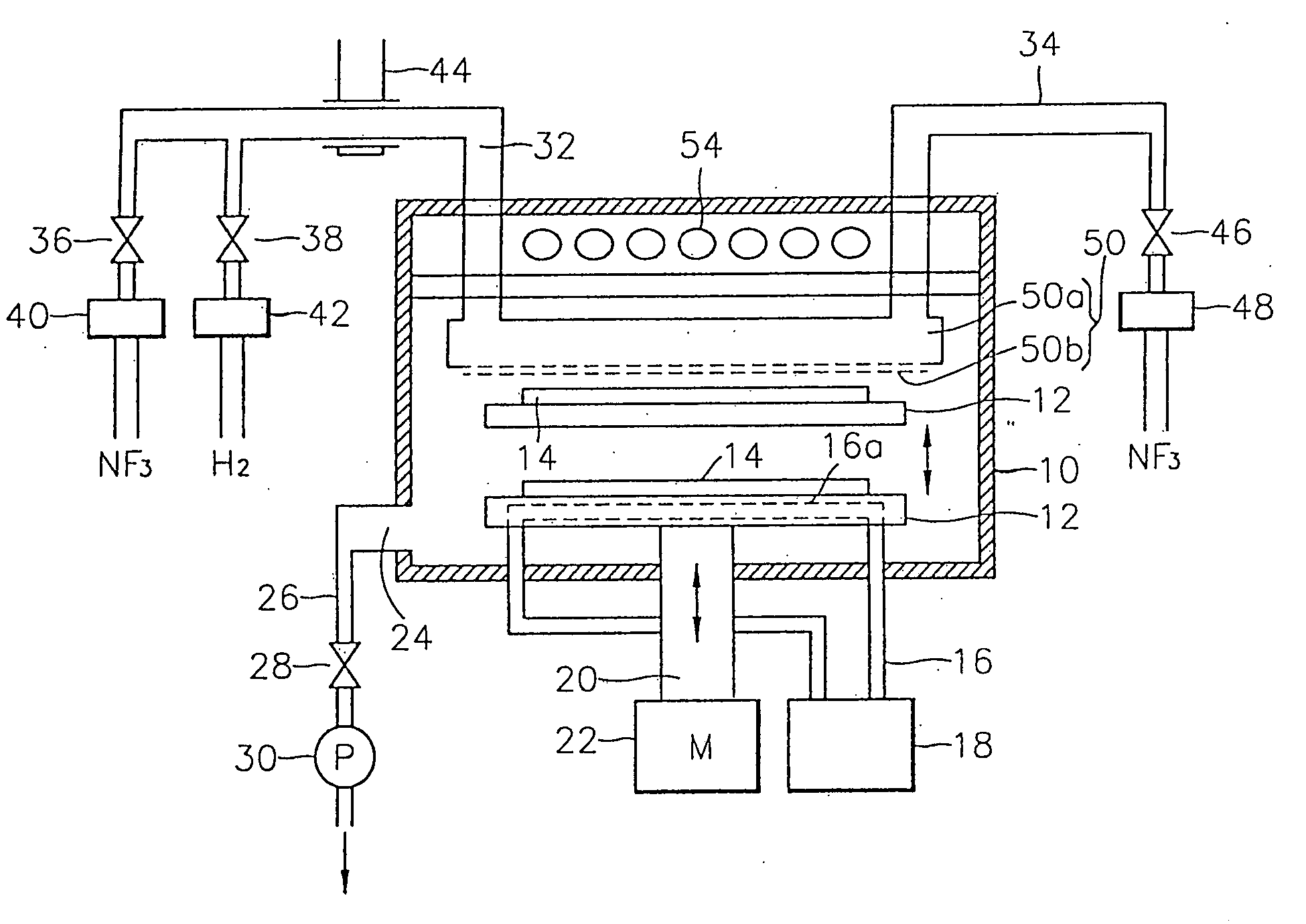
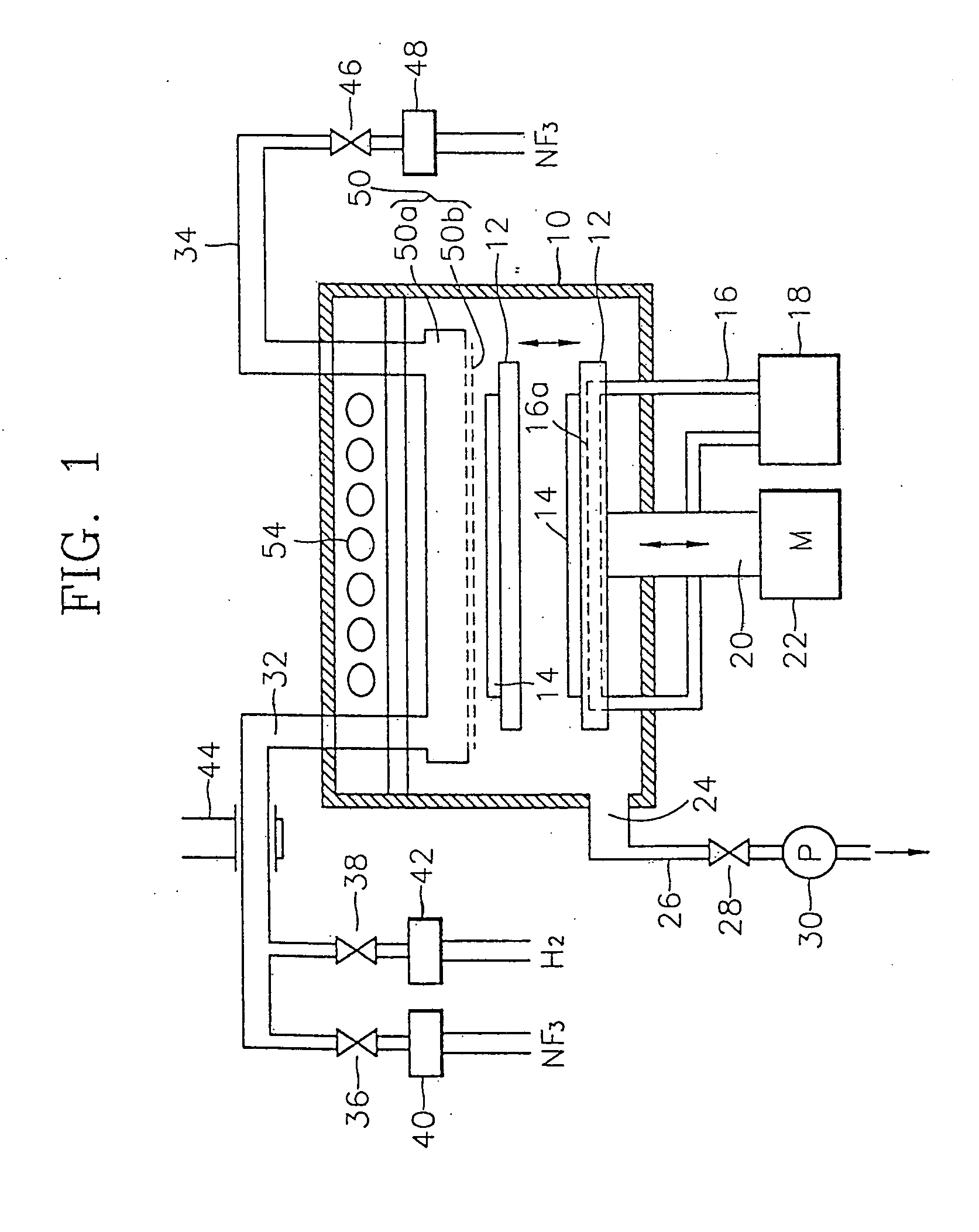
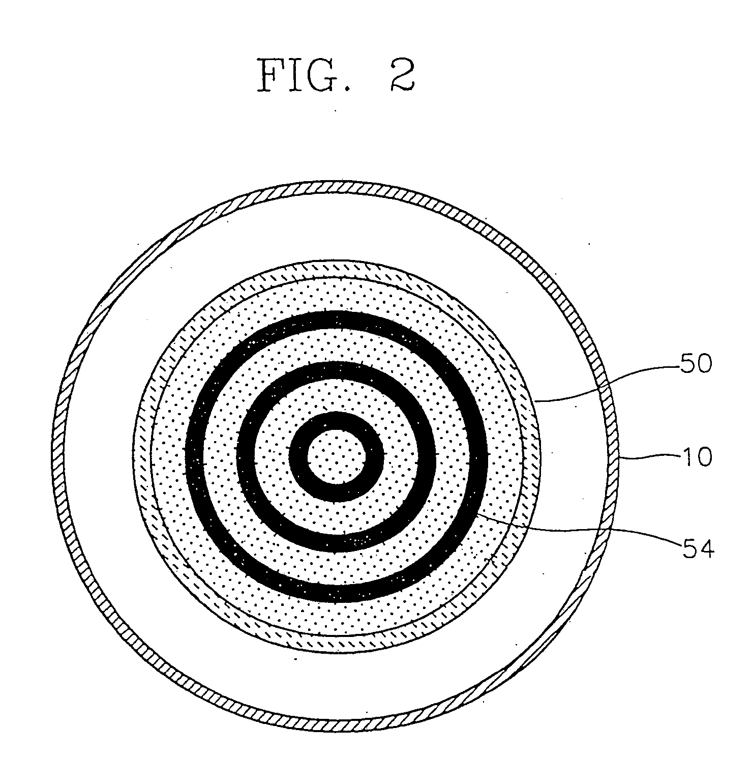
[0047] Referring to FIG. 1, an example of a semiconductor manufacturing apparatus which uses the embodiment of the oxide layer removing method according to the present invention is shown. The semiconductor manufacturing apparatus of FIG. 1 includes a vacuum chamber 10 which provides a vacuum condition, a plasma generating device 44 for producing plasma from reaction gases, a gas diffuser 50, a heater 54 installed to allow a continuous annealing process in the same chamber, a susceptor driving unit, which includes a susceptor 12, a shaft 20 and a motor M (22), for adjusting the location of a silicon wafer 14 in the vacuum chamber 10.

[0048] In particular, the susceptor 12, on which the silicon wafer 14 having an oxide layer to be etched is mounted, is installed in a lower central portion of the vacuum chamber 10. The susceptor 12, supported by the vertically movable shaft 20, moves upward and downward in the direction indic...


PUM

PropertyMeasurementUnit
Volumeaaaaaaaaaa
Ratioaaaaaaaaaa

Abstract

A method for removing an oxide layer such as a natural oxide layer and a semiconductor manufacturing apparatus which uses the method to remove the oxide layer. A vertically movable susceptor is installed at the lower portion in a processing chamber and a silicon wafer is loaded onto the susceptor when it is at the lower portion of the processing chamber. The air is exhausted from the processing chamber to form a vacuum condition therein. A hydrogen gas in a plasma state and a fluorine-containing gas are supplied into the processing chamber to induce a chemical reaction with the oxide layer on the silicon wafer, resulting in a reaction layer. Then, the susceptor is moved up to the upper portion of the processing chamber, to anneal the silicon wafer on the susceptor with a heater installed at the upper portion of the processing chamber, thus vaporizing the reaction layer. The vaporized reaction layer is exhausted out of the chamber. The oxide layer can be removed with a high selectivity while avoiding damage or contamination of the underlying layer.

Description

BACKGROUND OF THE INVENTION [0001] 1. Field of the Invention [0002] The present invention relates to a method of manufacturing semiconductor devices, and more particularly, to a method of eliminating an oxide layer such as a natural oxide layer, and a semiconductor manufacturing apparatus for use in the removal of the oxide layer. [0003] 2. Description of the Related Art [0004] Silicon wafers are susceptible to react with oxygen or moisture in the air, and thus a silicon dioxide (SiO2) layer, which deteriorates the characteristics of a semiconductor device, is formed on the surface of a silicon wafer by spontaneous oxidation. For example, if such a natural oxide layer is formed on the surface of contacts, contact resistance increases. Also, if a natural oxide layer is formed before growth of a gate oxide layer, the characteristics of the gate oxide layer can be altered or deteriorated. [0005] The most popular method used to remove a natural oxide layer in semiconductor fabrication i...

Claims


Application Information

Patent Timeline
IPC IPC(8): H01L21/302H01L21/306H01L21/3065H01L21/31H01L21/311
CPCH01L21/31116H01L21/02057H01L21/31
Inventor CHUNG, SEUNG-PILCHANG, KYU-WHANLEE, SUN-JUNGLEE, KUN-TACKPARK, IM-SOOLEE, KWANG-WOOKLEE, MOON-HEE
Owner SAMSUNG ELECTRONICS CO LTD
Why Eureka
Try Eureka