

CMOS image sensor and method for fabricating the same
a technology of image sensor and manufacturing method, which is applied in the field of cmos image sensor, can solve the problems of high power consumption, complicated driving method, and charge coupled device (ccd), and achieve the effect of reducing the darkcurrent and reducing the darkcurrent of the cmos image sensor
- Summary
- Abstract
- Description
- Claims
- Application Information
AI Technical Summary
Benefits of technology
Problems solved by technology
Method used
Image

Examples
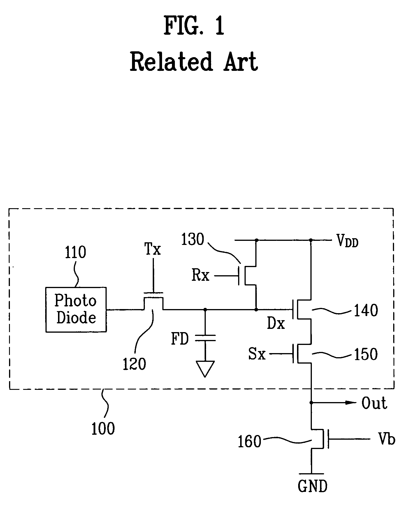
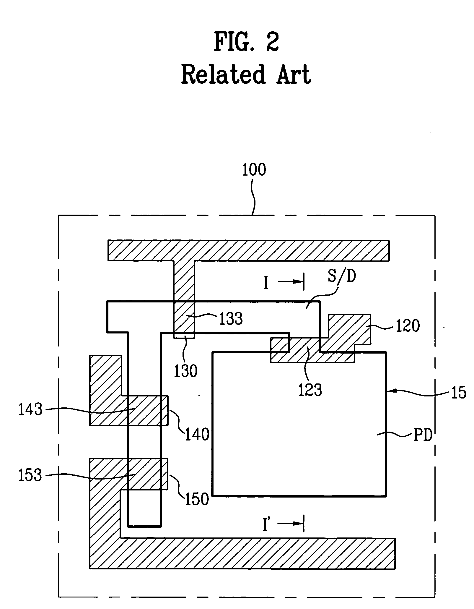
first embodiment
[0070]FIG. 5 is a cross sectional view of the photodiode along II-II′ of FIG. 4 according to the present invention.
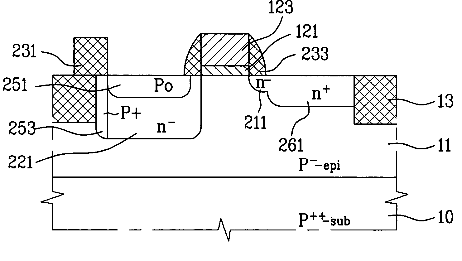
[0071] In the CMOS image sensor according to the first embodiment of the present invention, as shown in FIG. 5, a P− type epitaxial layer 11 is formed on a P++ type semiconductor substrate 10. The semiconductor substrate 10 may be formed of a crystal silicon substrate. To define and active area, a device isolation layer 13 is formed in a device isolation area of the semiconductor substrate 10. The device isolation layer 13 is formed in an STI (shallow trench isolation) process or an LOCOS (local oxidation of silicon) process. In this structure, a gate insulating layer 121 and a gate 123 are formed on the active area of the epitaxial layer 11 for the transfer transistor 140 of FIG. 4. Then, insulating layers 233 are formed at both sidewalls of the gate 123.
[0072] After that, an n− type diffusion area 221 and a P° type diffusion area 251 are formed in the epitaxial layer...
second embodiment
[0089] In the CMOS image sensor according to the present invention, as shown in FIG. 7, a P− type epitaxial layer 11 is formed on a P++ type semiconductor substrate 10. The semiconductor substrate 10 may be formed of a crystal silicon substrate. To define an active area, a device isolation layer 13 is formed in a device isolation area of the semiconductor substrate 10. The device isolation layer 13 may be formed in an STI (shallow trench isolation) process or an LOCOS (local oxidation of silicon) process. In this structure, a gate insulating layer 121 and a gate 123 are formed in the active area of the epitaxial layer 11 for the respective transistors explained in FIG. 4. Then, sidewall insulating layers 233 are formed at both sidewalls of the gate 123.
[0090] After that, an n− type diffusion area 221 and a P° type diffusion area 251 are formed in the epitaxial layer 11 of a photodiode PD. The P° type diffusion area 251 is formed on the n− type diffusion area 221. Also, source / drain ...
third embodiment
[0104] In the CMOS image sensor according to the present invention, as shown in FIG. 9, a P− type epitaxial layer 11 is formed on a P++ type semiconductor substrate 10. The semiconductor substrate 10 may be formed of a crystal silicon substrate. To define an active area, a device isolation layer 406a is formed in a device isolation area of the semiconductor substrate 10. The device isolation layer 406a is formed to have a higher surface than that of the epitaxial layer 11. In this structure, a gate insulating layer 121 and a gate 123 are formed in the active area of the epitaxial layer 11 for the transfer transistor 120, the reset transistor 130, the drive transistor 140, and the select transistor 150 explained in FIG. 4. Also, sidewall insulating layers 233 are formed at both sidewalls of the gate 123.
[0105] After that, an n− type diffusion area 221 and a P° type diffusion area 251 are formed in the epitaxial layer 11 of a photodiode PD. The P° type diffusion area 251 is formed on ...
PUM
 Abstract
Description
Claims
Application Information