

Method for depositing metallic nitride series thin film
a technology of metallic nitride and thin film, which is applied in the direction of coatings, solid-state devices, chemical vapor deposition coatings, etc., can solve the problems of deteriorating electrical characteristics, particularly severe design rules, and down and high density integration of devices
- Summary
- Abstract
- Description
- Claims
- Application Information
AI Technical Summary
Benefits of technology
Problems solved by technology
Method used
Image

Examples
Embodiment Construction
[0049] Referring now to the accompanying drawings, the preferred embodiments of the present invention will be described in detail below.
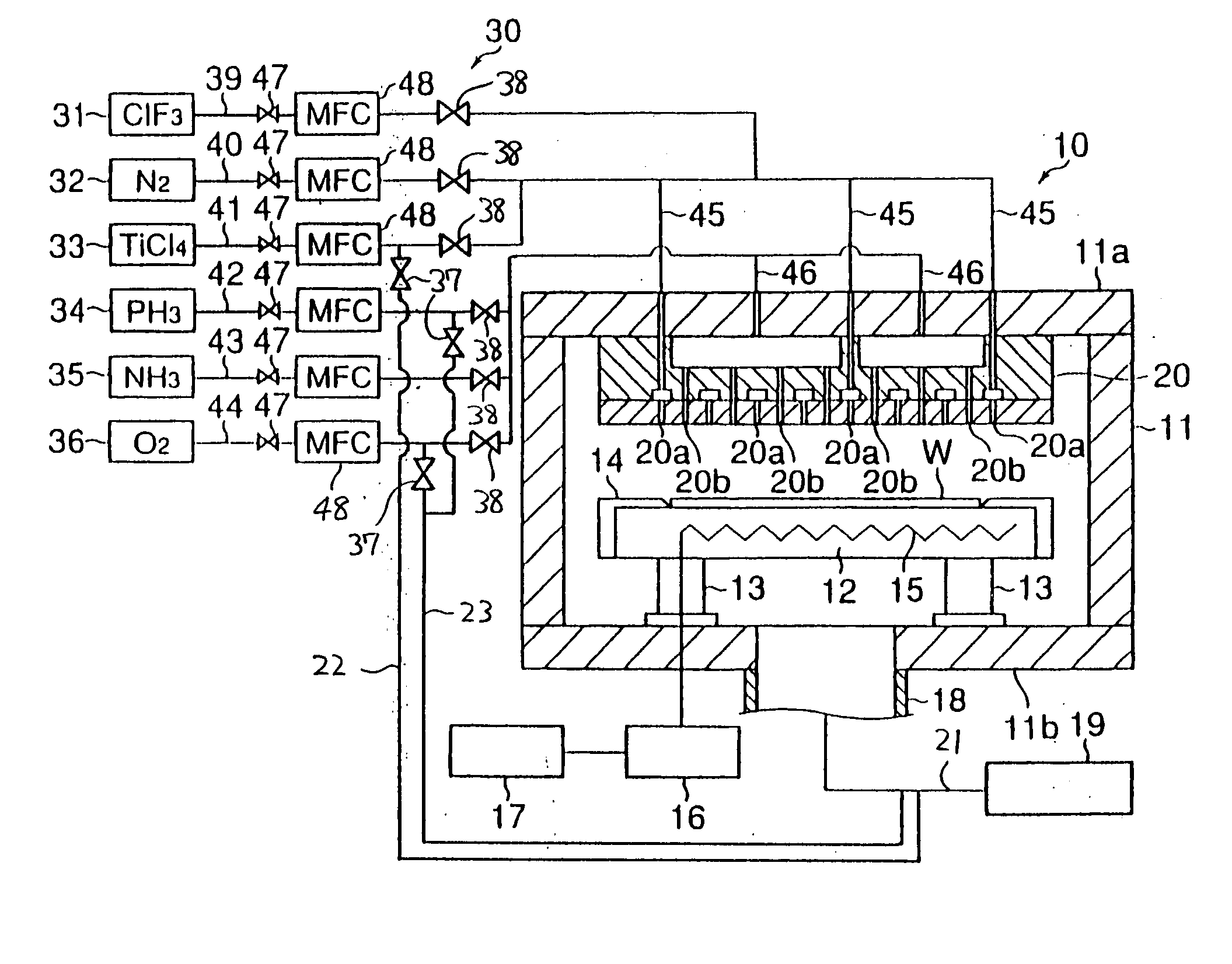
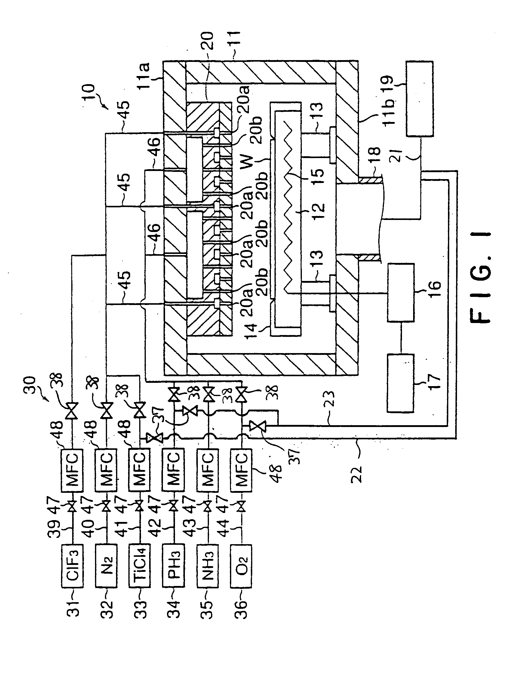
[0050]FIG. 1 is a sectional view of a deposition system for depositing a TiN-series thin film according to the present invention. This deposition system has a substantially cylindrical airtight process vessel 11, in which a susceptor 12 for horizontally supporting a semiconductor wafer W serving as an object to be processed is arranged while being supported on a cylindrical supporting member 13. On the outer edge portion of the susceptor 12, a guide ring 14 for guiding the semiconductor wafer W is provided. In addition, a heater 15 is embedded in the susceptor 12. When an electrical power is fed to the heater 15 from a power supply 16, the heater 15 heats the semiconductor waver W, which is an object to be processed, to a predetermined temperature. The power supply 16 is connected to a controller 17 which controls the output of the heater 15 in acc...
PUM
| Property | Measurement | Unit |
|---|---|---|
| temperature | aaaaa | aaaaa |
| pressure | aaaaa | aaaaa |
| pressure | aaaaa | aaaaa |
Abstract
Description
Claims
Application Information