Organic electro-optic device and method for making the same

Active Publication Date: 2005-05-05
BOE TECH GRP CO LTD
View PDF6 Cites 72 Cited by
  • Summary
  • Abstract
  • Description
  • Claims
  • Application Information

AI Technical Summary

Problems solved by technology
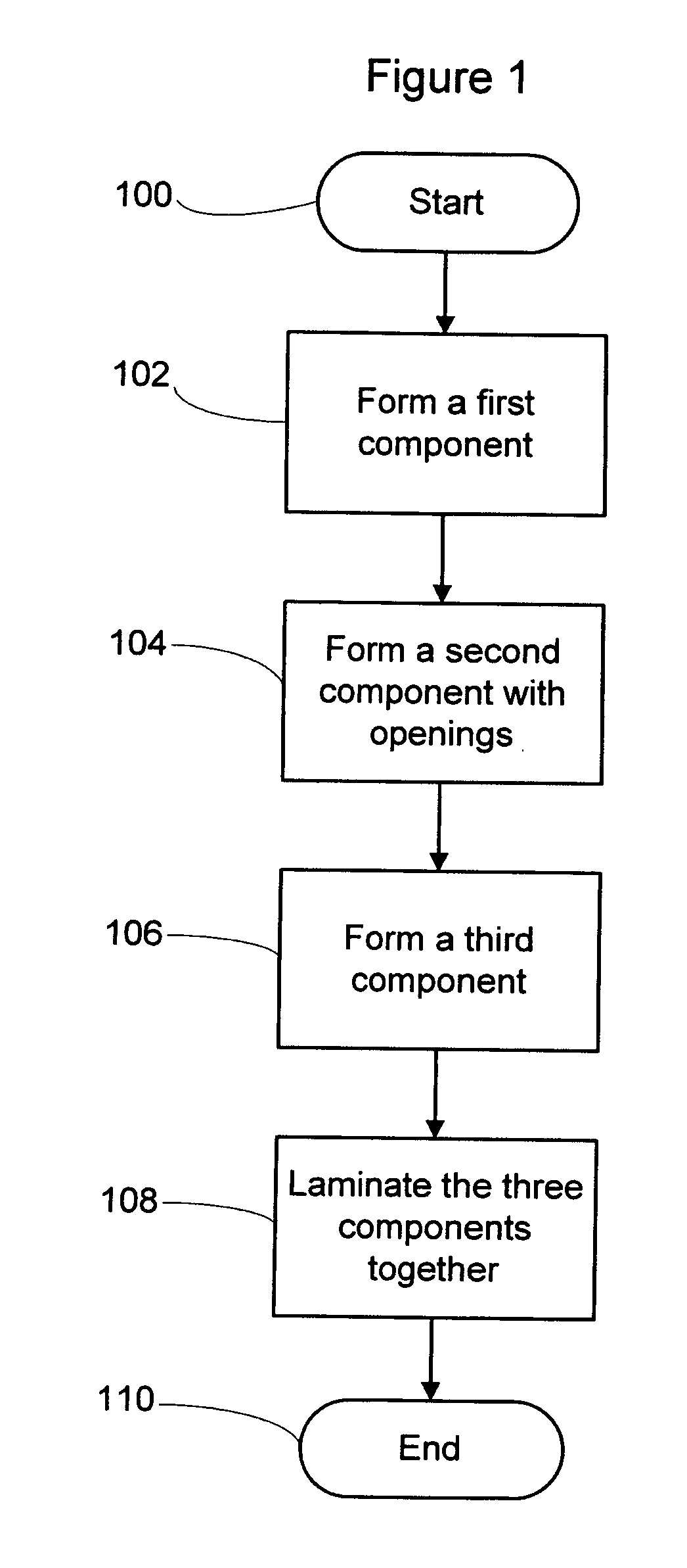
A number of disadvantages exist with this manufacturing approach, however.
The presence of vacuum processes greatly increases the cost of the much desired roll-to-roll (R2R) process where a roll of substrate can be continuously converted into a roll of product.
In addition, since the cathode metal and active materials in an OLED are sensitive to air and water vapor and degrade rapidly if left unpackaged, it is often necessary to encapsulate tradition

Method used


Image

  • Organic electro-optic device and method for making the same
  • Organic electro-optic device and method for making the same
  • Organic electro-optic device and method for making the same

Examples


example 1

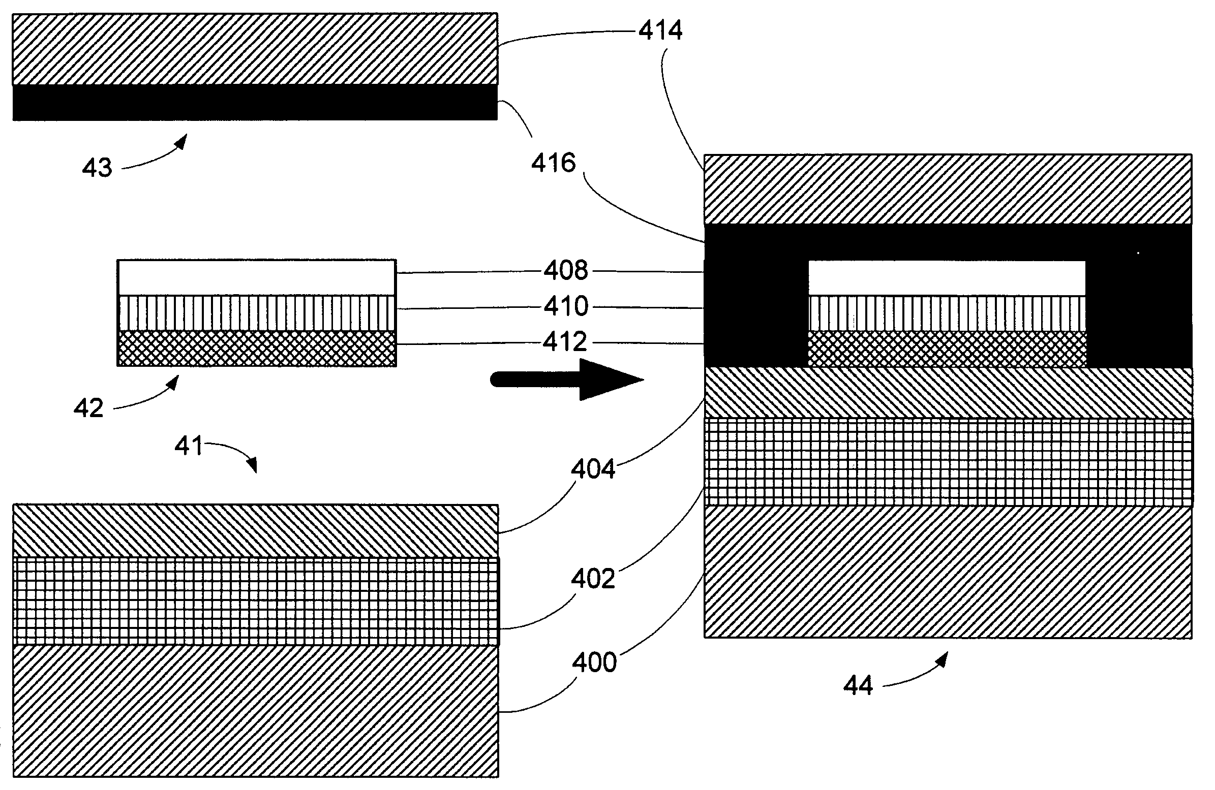
[0045] An OLED device was formed as follows. A first component comprised a polyethylene terephthalate (PET) substrate coated with an ITO layer and a PEDOT layer. A second component comprised a PET substrate coated with an ITO layer and a layer of polymer blend in which an emissive polymer, ADS329 (Poly(9,9-dioctylfluorenyl-2,7-diyl), purchased from American Dye Source, Inc. (555 Morgan Boulevard, Baie D.Urfe, Quebec, Canada H9X 3T6), was blended with an adhesive material, Norland Optical Adhesive 68 (“Norland 68”), purchased from Norland Products, Inc. (Cranbury, N.J. 08512, U.S.A.). The first component thus had a structure of PET / ITO / PEDOT and the second component had a structure of PET / ITO / (polymer blend). These two components were subsequently laminated together followed by a short (30 seconds) exposure to UV irradiation. Before lamination, photoluminescence was only observed (due to ADS329) from the second component. After lamination, the laminated film was separated on purpose....

example 2

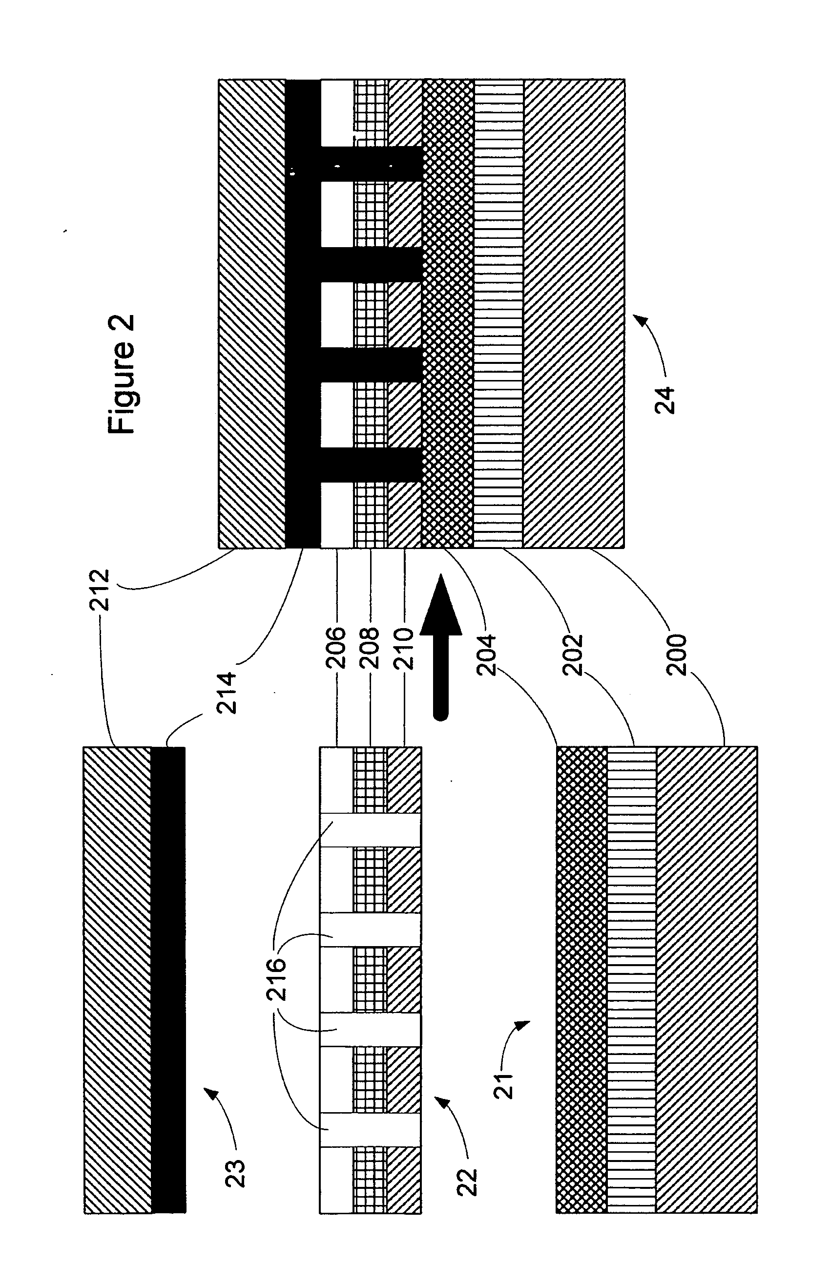
[0046] In another experiment, two working devices with a structure of PET / ITO / PEDOT / (polymer blend) / Al / PET were made via lamination of separate components, wherein Al was an aluminum cathode layer and the polymer blend comprised a blend of ADS329 and Norland 68. The first device was made using a component with a structure of PET / ITO / PEDOT / (polymer blend) and a component with a structure of PET / Al. The second device was made using a component with a structure of PET / ITO / PEDOT and a component with a structure of PET / Al / (polymer blend). The polymer blend layer was spin-coated and the laminated film stacks were cured using a long wavelength (365 nm) UV-lamp for five minutes in air. Both devices showed enhanced mechanical properties, i.e. strengthened adhesion between the PEDOT and the emissive polymer, as well as between the emissive polymer and the Al cathode.

example 3

[0047] In another example, emissive polymer ADS329 was mixed with adhesive material Norland 68. The blend solution was prepared by mixing 52 milligrams of ADS329 with 19 milligrams of degassed Norland 68 in an amber vial at room temperature in air, purging the mixture in nitrogen for 40 minutes, adding 4 milliliters of M-xylene (anhydrous), heating the solution at 75° C. (stirring with a stir bar) for one hour and cooling down to room temperature in a nitrogen-purged box. An organic light emitting device (“Device A”) was fabricated following the steps of: (1) spin-coating PEDOT onto a pre-cleaned, UV-ozoned ITO substrate; (2) baking the ITO / PEDOT substrate at 170° C. for 30 minutes and then cooling it down to room temperature in a nitrogen-purged box; (3) spin-coating the blend solution, as prepared above, onto the ITO / PEDOT substrate, then partially curing it with a long-wavelength (365 nm) UV-lamp for 30 seconds; (4) transferring the sample into an argon-purged box (moisture and o...


PUM

PropertyMeasurementUnit
Temperatureaaaaaaaaaa
Timeaaaaaaaaaa

Abstract

The present invention directed to an organic light emitting device and method for making the same. The method comprises the steps of: forming a first component comprising at least one first material on a first substrate; forming a second component comprising at least one second material on a second substrate, wherein at least one opening is formed through the second component; forming a third component; and laminating the first component, the second component and the third component together such that the second component is located between the first component and the third component, the at least one first material and the at least one second material form at least part of an organic electro-optic device located between the first substrate and the second substrate, the third component is bonded to the second component, and the third component is bonded to the first component through the at least one opening.

Description

BACKGROUND OF THE INVENTION [0001] The present invention relates generally to the field of electro-optics, and more particularly to an organic electro-optic device and method for making the same. [0002] Organic electro-optic devices include organic light emitting devices (OLEDs) and organic photovoltaic devices, for example. An OLED typically comprises one or more semi-conducting organic thin films sandwiched between two electrodes, one of which is usually transparent. When a forward bias is applied, injected electrons and holes recombine in the organic layers to generate light. Organic light emitting devices have great potential in the display and lighting industry. Due to their increased brightness, faster response time, lighter weight and lower power consumption, OLED displays are expected to replace liquid crystal display (LCD) applications in the near future. [0003] Another type of organic electro-optic device is a photovoltaic device. A photovoltaic cell typically comprises a ...

Claims


Application Information

Patent Timeline
IPC IPC(8): H01L27/32H01L51/00H01L51/30H01L51/40H01L51/50H01L51/52H01L51/56
CPCH01L27/3202H01L27/3204H01L51/0024H01L51/0037H01L51/0038Y02E10/549H01L51/5036H01L51/5203H01L51/5268H01L51/56H01L51/0039Y10T428/31504Y02P70/50H10K59/84H10K59/86H10K71/50H10K85/114H10K85/115H10K85/1135H10K50/125H10K50/805H10K50/854H10K71/00H05B33/10
Inventor LIU, JIDUGGAL, ANIL RAJ
Owner BOE TECH GRP CO LTD
Why Eureka
Try Eureka