Organic electroluminescence device and method of manufacture

Inactive Publication Date: 2005-05-05
IBM CORP
View PDF3 Cites 65 Cited by
  • Summary
  • Abstract
  • Description
  • Claims
  • Application Information

AI Technical Summary

Benefits of technology

[0012] It is an aspect of the present invention to provide a further extension of life of the dye for the organic EL device which is added in the light emitting layer and gives light emission with a desired wa

Problems solved by technology

Moreover, the device lifetime is reduced also by degradation of the dye itself.
However, the various resear

Method used


Image

  • Organic electroluminescence device and method of manufacture
  • Organic electroluminescence device and method of manufacture
  • Organic electroluminescence device and method of manufacture

Examples


examples

[0059] Hereinafter, the present invention will be described with specific examples. The present invention is not limited by examples described later. Table 2 shows compositions used in the examples.

examples 1 to 4

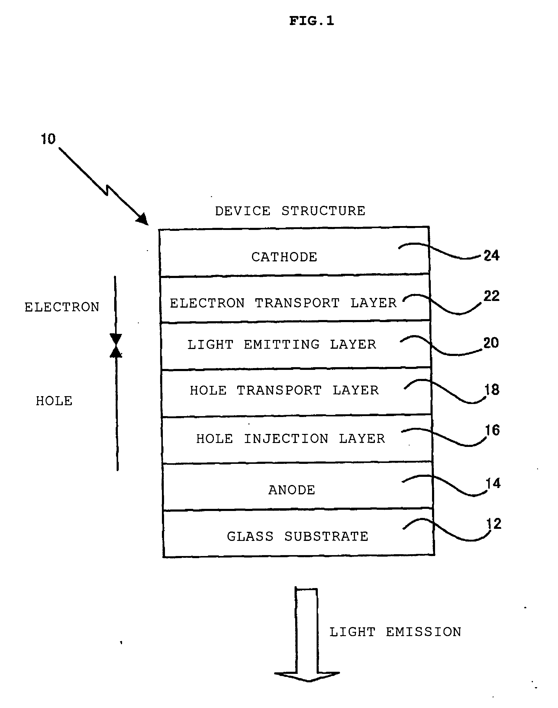
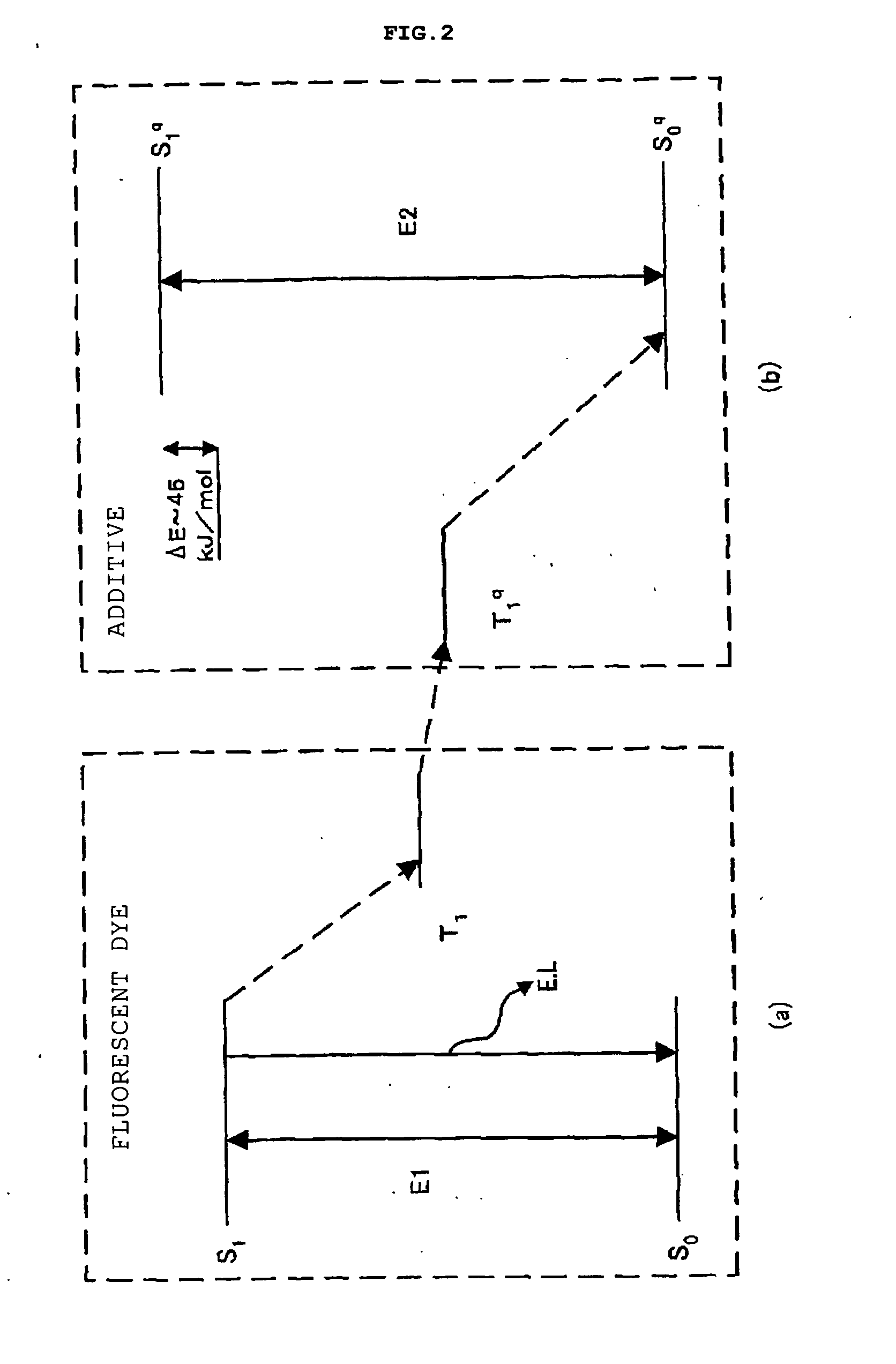
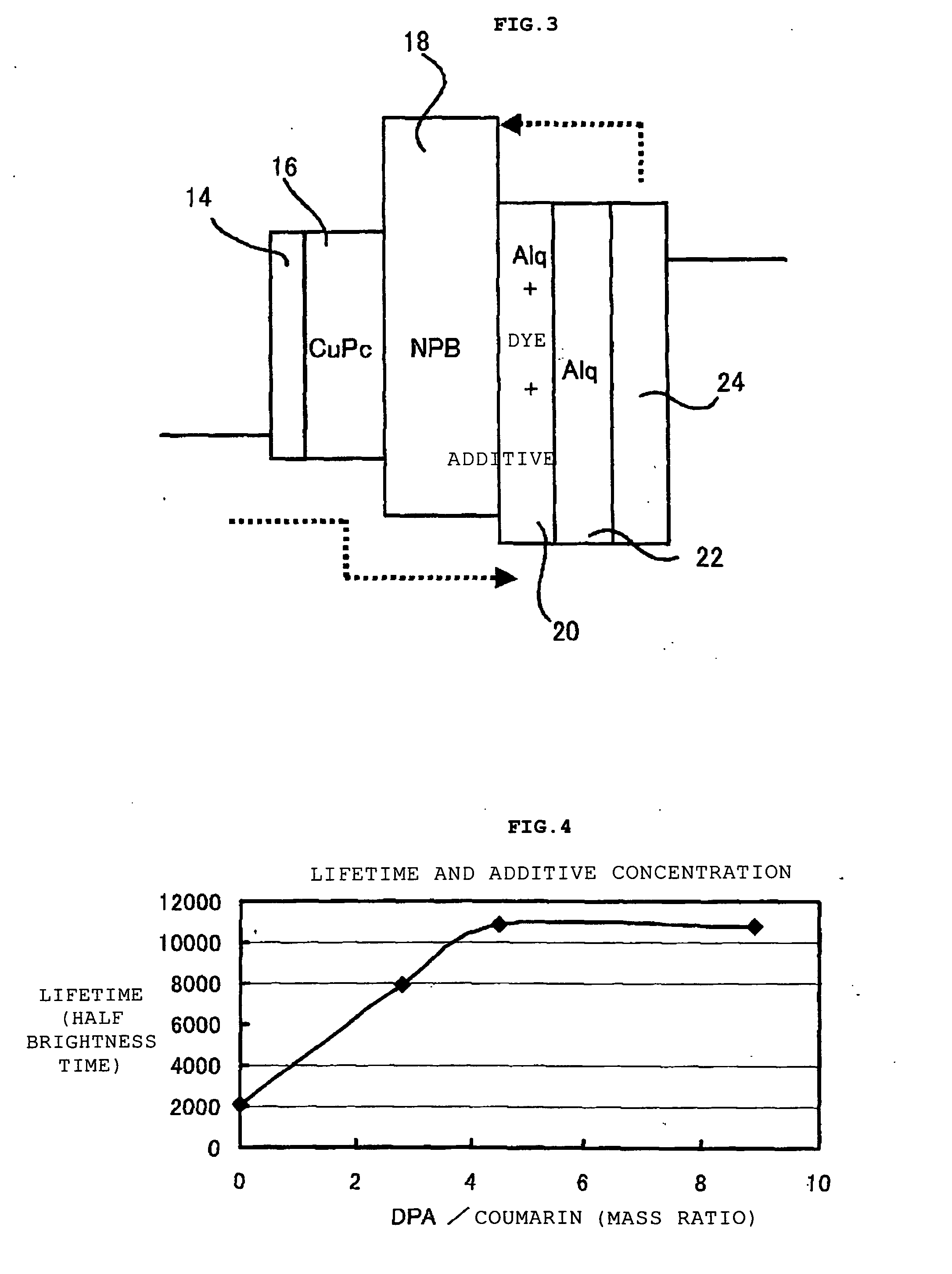
[0060] Organic EL devices were formed as shown in FIG. 3. Each organic EL device shown in FIG. 3 was produced in the following manner. First, copper phthalocyanine was evaporated as the hole injection layer to a thickness of 10 nm on a glass substrate with an ITO film deposited as the anode. α-NPB was then deposited thereon to form the hole transport layer with a thickness of 30 nm. On the formed hole transport layer, Alq3, 1 mass % of coumarin 6, and about 3, 5, or 9 mass % or none of 9,10-diphenylanthracene (DPA) to be the triplet quencher were evaporated from different sources and were deposited into the light emitting layer with a thickness of 30 nm. Subsequently, Alq3 was deposited thereon to form an electron injection layer with a thickness of 30 nm. After LiF was evaporated to about 0.5 nm, Al was evaporated to form the cathode with a thickness of 200 nm. Lead lines are attached to the anode and cathode of the produced organic EL device by using silver paste and connected to ...

examples 5 to 8

[0065] Similar experiment was carried out with the amounts of dye and additive changed as shown in Table 2, and good results were obtained.

[0066] As described above, according to the present invention, the luminescence lifetime of the organic EL device can be increased, and it is possible to provide an organic EL device with longer lifetime and good display properties.

TABLE 2S1AddedS1AddedEnergyAmountEnergyAmountExampleDye(kJ / mol)(mass %)Additive(kJ / mol)(mass %)Example 1coumarin 626019,10-diphenylanthracene3040Example 2coumarin 619,10-diphenylanthracene3Example 3coumarin 619,10-diphenylanthracene5Example 4coumarin 619,10-diphenylanthracene9Example 5rhodamine1811rubrene22136GExample 6rhodamine1rubrene56GExample 75,7-dimethoxycoumarin33912-naphthyl2′-3591naphthaleneExample 85,7-dimethoxycoumarin12-naphthyl2′-2naphthalene


PUM

PropertyMeasurementUnit
Bond energyaaaaaaaaaa
Absorption edgeaaaaaaaaaa

Abstract

An organic electroluminescence device of the present invention comprises a light emitting layer held between electrodes, the light emitting layer containing at least a host material and a dye or pigment. The light emitting layer further comprises an additive exhibiting an absorption edge of which energy level is higher than that of an absorption edge of the dye or pigment, but the difference of the energy levels being less than 120 kJ/mol, having no lone pair, and including at least two aromatic rings. The additive of the present invention is selected from a group consisting of phenyl-substituted anthracenes, naphthyl-substituted anthracenes, naphthyl-substituted naphthalenes, pyrenes, and a naphthacene derivatives.

Description

FIELD OF THE INVENTION [0001] The present invention relates to an organic electroluminescence device. Specifically, the present invention relates to an organic electroluminescence device with longer lifetime and improved display properties by improving organic electroluminescence lifetime and relates to a method of manufacturing the organic electroluminescence device. BACKGROUND OF THE INVENTION [0002] An organic electroluminescence (EL) device is a self-emitting device with very fast response. Applying the organic EL device to a display device can be expected to provide a good flat display device with wide viewing angle. Therefore, the organic EL device has been studied to be applied to flat display devices which are to be replaced for liquid crystal displays. [0003] On the contrary, it has been known that the organic EL device has various disadvantages, and various researches have been given thereto. Especially, researches have been carried out from the perspective of the device c...

Claims


Application Information

Patent Timeline
IPC IPC(8): C09K11/06H01L51/50H01L51/00H05B33/10H05B33/14
CPCC09K11/06C09K2211/1011H01L51/0052H01L51/0059H05B33/14H01L51/0078H01L51/0081H01L51/5012H01L51/0062H10K85/649H10K85/615H10K85/631H10K85/311H10K85/324H10K50/11
Inventor TAKEDA, KEIZO
Owner IBM CORP
Why Eureka
Try Eureka