Liquid crystal display device including polycrystalline silicon thin film transistor and method of fabricating the same

a thin film transistor and liquid crystal display technology, applied in static indicating devices, instruments, non-linear optics, etc., can solve the problems of deteriorating the stability of tft, reducing the production cost, and not using tft using hydrogenated amorphous silicon for driving circuits, etc., to achieve the effect of increasing production yield and reducing production costs

Active Publication Date: 2005-05-12
LG DISPLAY CO LTD
View PDF5 Cites 42 Cited by
  • Summary
  • Abstract
  • Description
  • Claims
  • Application Information

AI Technical Summary

Benefits of technology

[0027] Another object of the present invention is to provide an LCD device where a produc...

Problems solved by technology

In hydrogenated amorphous silicon, however, since atoms are randomly arranged, weak bonds and dangling bonds exist.
Accordingly, when light is irradiated or an electric field is applied, the hydrogenated amorphous silicon has a quasi-static state and this quasi-static state may deteriorate the stability of the TFT.
Furthermore, the TFT using hydrogenated amorphous sil...

Method used


Image

  • Liquid crystal display device including polycrystalline silicon thin film transistor and method of fabricating the same
  • Liquid crystal display device including polycrystalline silicon thin film transistor and method of fabricating the same
  • Liquid crystal display device including polycrystalline silicon thin film transistor and method of fabricating the same

Examples


Embodiment Construction

[0044] Reference will now be made in detail to a preferred embodiment of the present invention, examples of which are shown in the accompanying drawings. Wherever possible, similar reference numbers will be used throughout the drawings to refer to the same or similar parts.

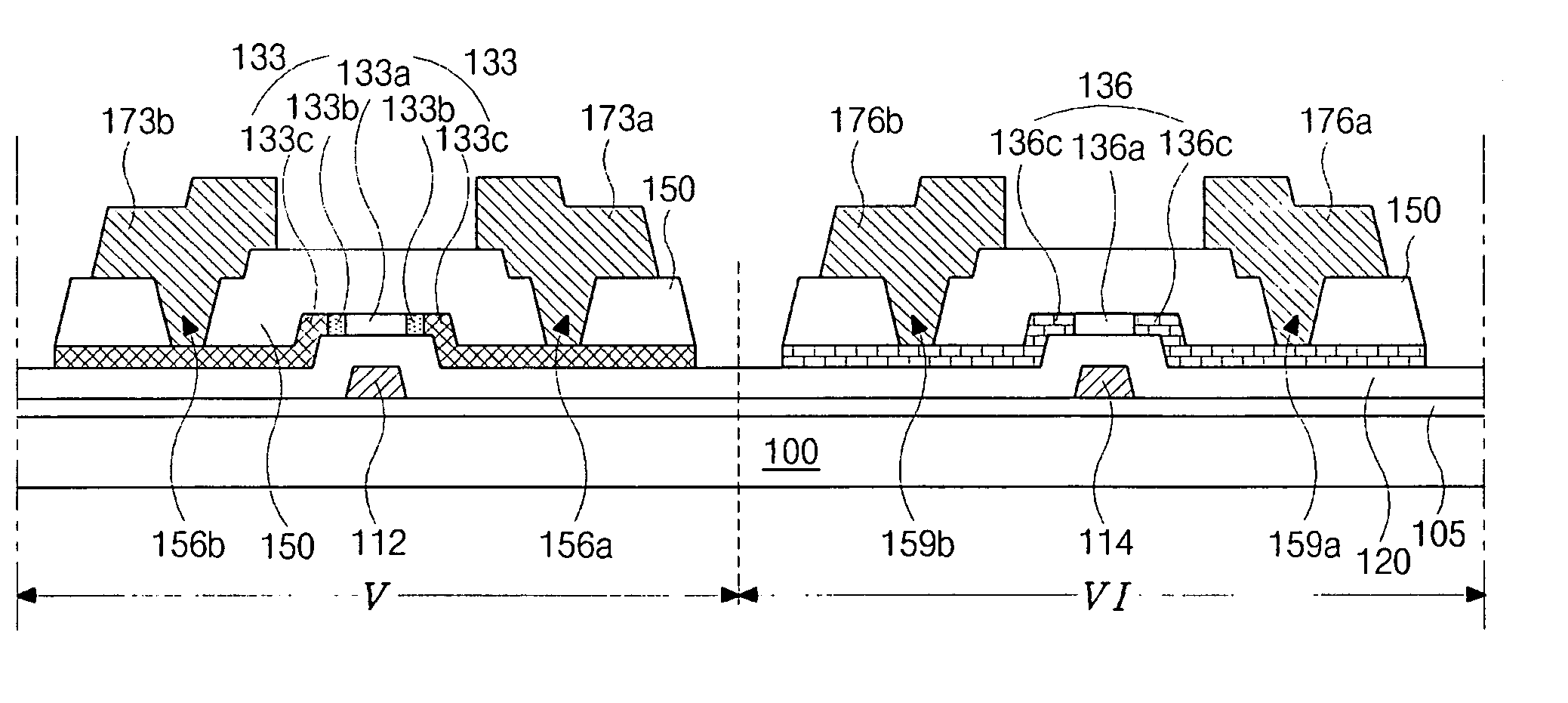
[0045]FIG. 5A is a schematic cross-sectional view showing a switching element in a pixel portion of an array substrate for a liquid crystal display device according to an embodiment of the present invention and FIG. 5B is a schematic cross-sectional view showing CMOS switching elements in a driving portion of an array substrate for a liquid crystal display device according to an embodiment of the present invention.

[0046] As shown in FIG. 5A, a buffer layer 105 is formed on a substrate 100. The buffer layer 105 may be formed of an inorganic insulating material, such as silicon nitride (SiNx) or silicon oxide (SiO2). A first gate electrode 110 is formed on the buffer layer 105. The first gate electrode 110 may be ...


PUM


Abstract

A liquid crystal display device having a switching element in a pixel portion and a CMOS element in a driving portion includes: a substrate; a gate electrode on the substrate; a gate insulating layer on the gate electrode; a polycrystalline silicon layer on the gate insulating layer, the polycrystalline silicon layer having an active region in a central portion corresponding to the gate electrode and an ohmic contact region at side portions of the active region; an interlayer insulating layer having a set of contact holes for contacting the polycrystalline silicon layer at the side portions; and source and drain electrodes spaced apart from each other on the interlayer insulating layer, the source and drain electrodes contacting the polycrystalline silicon layer through the set of contact holes.

Description

[0001] This application claims the benefit of Korean Patent Application No. 2003-0079289, filed on Nov. 11, 2003, which is hereby incorporated by reference as if fully set forth herein. BACKGROUND OF THE INVENTION [0002] 1. Field of the Invention [0003] The present invention relates to a liquid crystal display device, and more particularly, it relates to a liquid crystal display (LCD) device including a polycrystalline silicon thin film transistor (p-Si TFT) and a method of fabricating the same. [0004] 2. Discussion of the Related Art [0005] Liquid crystal display (LCD) devices are being developed as the next generation of display devices because of their advantageous characteristics of light weight, thin profile, and low power consumption. In general, an LCD device is a non-emissive display device that displays images by making use of a refractive index difference through utilizing optical anisotropy properties of liquid crystal molecules interposed between an array substrate and a...

Claims


Application Information

Patent Timeline
IPC IPC(8): G02F1/133G09G3/36G02F1/136G02F1/1368G03F7/20H01L21/00H01L29/786
CPCG02F1/1368G09G3/36
Inventor YANG, MYOUNG-SUOH, KUM-MI
Owner LG DISPLAY CO LTD
Why Eureka
Try Eureka