Method of reducing dislocation-induced leakage in a strained-layer field-effect transistor

Inactive Publication Date: 2005-05-19
ALSEPHINA INNOVATIONS INC
View PDF10 Cites 8 Cited by
  • Summary
  • Abstract
  • Description
  • Claims
  • Application Information

AI Technical Summary

Benefits of technology

[0014] Advantageously, the device and fabricating method of the invention relaxes the requirement for reducing the threading d

Problems solved by technology

The threading and misfit dislocations can lead to device failure in a short-channel MOSFET fabricated on these layers particularly if the dislocation extends continuously from the source implant region to the drain implant region.
In this case, the dopants from the source and drain can segregate along the dislocation, causing a direct “pipe” from source to drain, resulting in device leakage.
Since larger atoms can preferentially occupy dislocation sites, n-MOSFETs are more likely to suffer from dislocation-related failures of the type described above.
The data shows that the leakage is seen to occur directly from source to drain (and not from source to body or drain to body, Ib), resulting in poor turn off behavior and high leakage 55 in the subthreshold region (Vgs<0).
Both of these methods have been successful in reducing dislocation-induced leakage, but it is very difficult to comp

Method used


Image

  • Method of reducing dislocation-induced leakage in a strained-layer field-effect transistor
  • Method of reducing dislocation-induced leakage in a strained-layer field-effect transistor
  • Method of reducing dislocation-induced leakage in a strained-layer field-effect transistor

Examples


Example

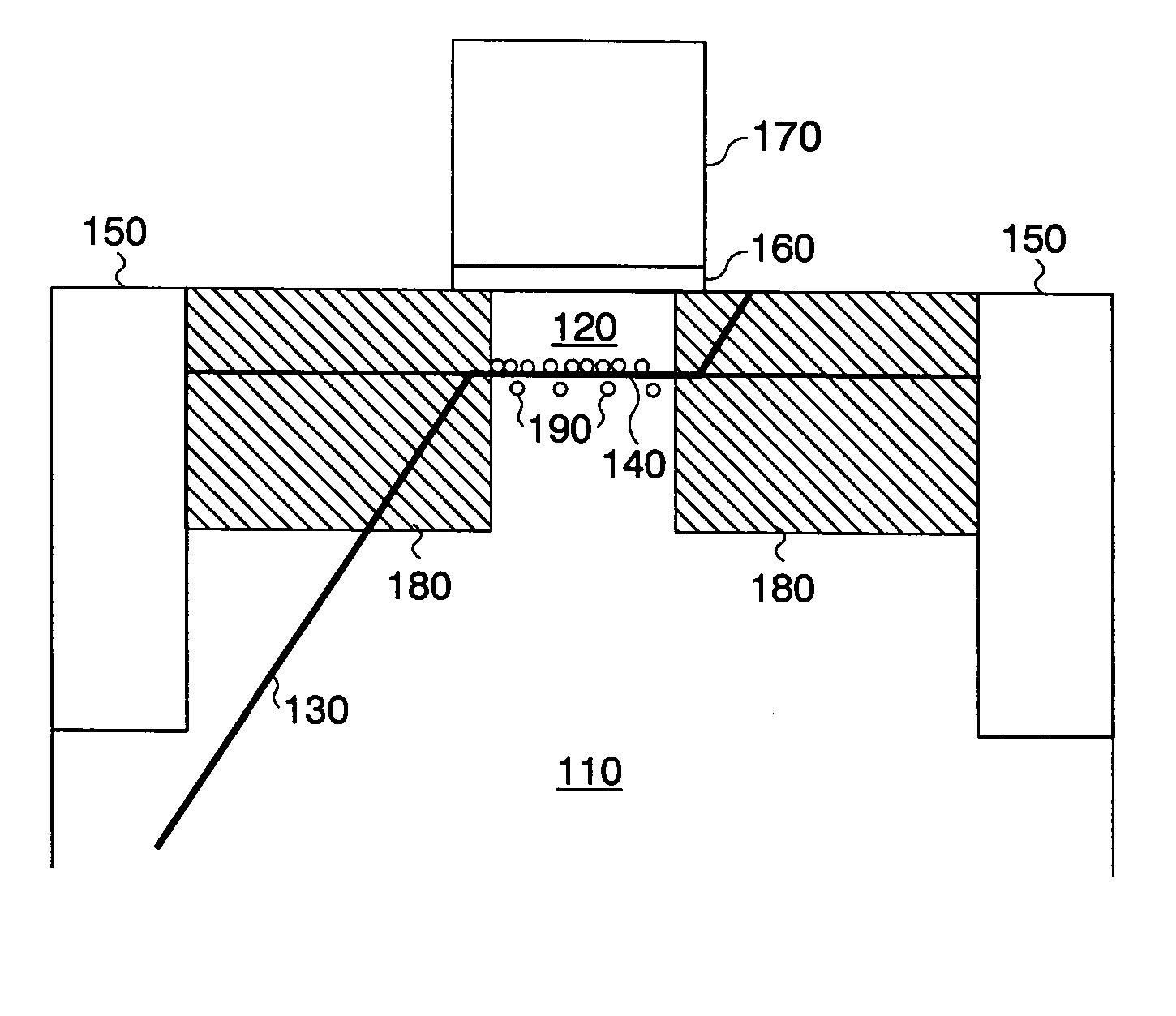
[0023]FIG. 3 is a cross-sectional diagram of a first embodiment of the invention showing a strained Si n-MOSFET where a defect spanning from source to drain is partially occupied by heavy p-type dopants. Preferably, the strained-layer n-MOSFET includes a Si, SiGe or SiGeC multi-layer structure consisting of these materials, that has, in the region between source and drain, impurity atoms that preferentially occupy the dislocation sites so as to prevent shorting of source and drain via dopant diffusion along the dislocation. Advantageously, devices formed as a result of the invention are immune to dislocation-related failures, and therefore are more robust to processing and material variations. This invention relaxes the requirement for reducing the threading dislocation density in SiGe buffers, since the devices will be operable despite the presence of a finite number of dislocations.

[0024] In the preferred embodiment of the strained Si n-MOSFET depicted in FIG. 3, indium, In, is u...

Example

[0025]FIG. 4 is a cross-sectional diagram of a second embodiment of the invention showing a strained Si p-MOSFET device 200 where a defect spanning from source to drain is partially occupied by heavy n-type dopants. This device has the same structure as in FIG. 3, except that the source and drain electrodes 220 are p-type doped with boron, B, for example, the regions 210 between and below the source and drain regions are doped n-type. In the embodiment of the strained Si p-MOSFET depicted in FIG. 4, antimony, Sb, is utilized as a blocking material for boron, B, diffusion along the dislocation. That is, the region of the dislocation between the source and drain regions is partially occupied by Sb atoms 230 that act to block segregation of the source and drain dopant atoms along the dislocation, thus preventing a short between source and drain.

Example

[0026]FIG. 5 is a cross-sectional diagram of a third embodiment of the invention showing a strained Si p-MOSFET device 300 having the same structure as either the device in FIG. 3 or FIG. 4. In the third embodiment, dislocation defect sites spanning from source to drain are partially occupied by neutral dopant species 360 that blocks segregation of the source and drain dopant atoms along the dislocation, thus preventing a short between source and drain implant regions. The advantage of neutral impurities is that they are less likely to affect the electrical properties of the device, and so higher doses could be used to more effectively passivate the device. In addition, the same dopant species may be used to passivate both nFETs and pFETs. The preferred candidates for neutral impurity passivation species are group IV impurities such as carbon, (C), tin (Sn) or lead (Pb), or a combination thereof. The implanted species may also form a complex with existing impurities in the semicondu...


PUM


Abstract

A structure and method of fabricating a semiconductor field-effect transistor (MOSFET) such as a strained Si n-MOSFET where dislocation or crystal defects spanning from source to drain is partially occupied by heavy p-type dopants. Preferably, the strained-layer n-MOSFET includes a Si, SiGe or SiGeC multi-layer structure having, in the region between source and drain, impurity atoms that preferentially occupy the dislocation sites so as to prevent shorting of source and drain via dopant diffusion along the dislocation. Advantageously, devices formed as a result of the invention are immune to dislocation-related failures, and therefore are more robust to processing and material variations. The invention thus relaxes the requirement for reducing the threading dislocation density in SiGe buffers, since the devices will be operable despite the presence of a finite number of dislocations.

Description

BACKGROUND OF THE INVENTION [0001] 1. Field of the Invention [0002] The present invention relates to semiconductors and transistors and more particularly to Si / SiGe strained-layer field-effect transistors. [0003] 2. Description of the Prior Art [0004] Semiconductor Si / SiGe strained-layer MOSFETs fabricated using strained Si have potential for improved performance due to higher carrier mobility in the strained Si layer. The strain in the Si is typically achieved by first forming a relaxed SiGe layer, and then epitaxially growing the Si layer on top. Since the SiGe has a larger lattice constant than Si, the Si will be under tensile strain. The underlying relaxed SiGe layer can be formed in numerous ways, but is typically formed by growing a graded-Ge-content SiGe layer on a Si substrate, followed by a thick constant-composition SiGe layer. The SiGe relaxes by misfit dislocation formation near the original growth interface, with a fairly high density (on the order of about 106 cm−2-108...

Claims


Application Information

Patent Timeline
IPC IPC(8): H01L21/265H01L21/335H01L29/10H01L29/51H01L29/76H01L29/772H01L29/78
CPCH01L21/26506H01L21/26513H01L29/1041H01L29/78H01L29/51H01L29/517H01L29/518H01L29/1054
Inventor KOESTER, STEVEN J.
Owner ALSEPHINA INNOVATIONS INC
Why Eureka
Try Eureka