

Method for forming a storage cell capacitor compatible with high dielectric constant materials
a storage cell capacitor and dielectric constant technology, applied in the field of semiconductor devices, can solve the problems of inability to simply deposited on a polysilicon electrode, memory devices cannot be made as dense, and incompatible with existing processes, so as to maximize die space, reduce the height of stack capacitors, and maximize cell size
- Summary
- Abstract
- Description
- Claims
- Application Information
AI Technical Summary
Benefits of technology
Problems solved by technology
Method used
Image

Examples
Embodiment Construction
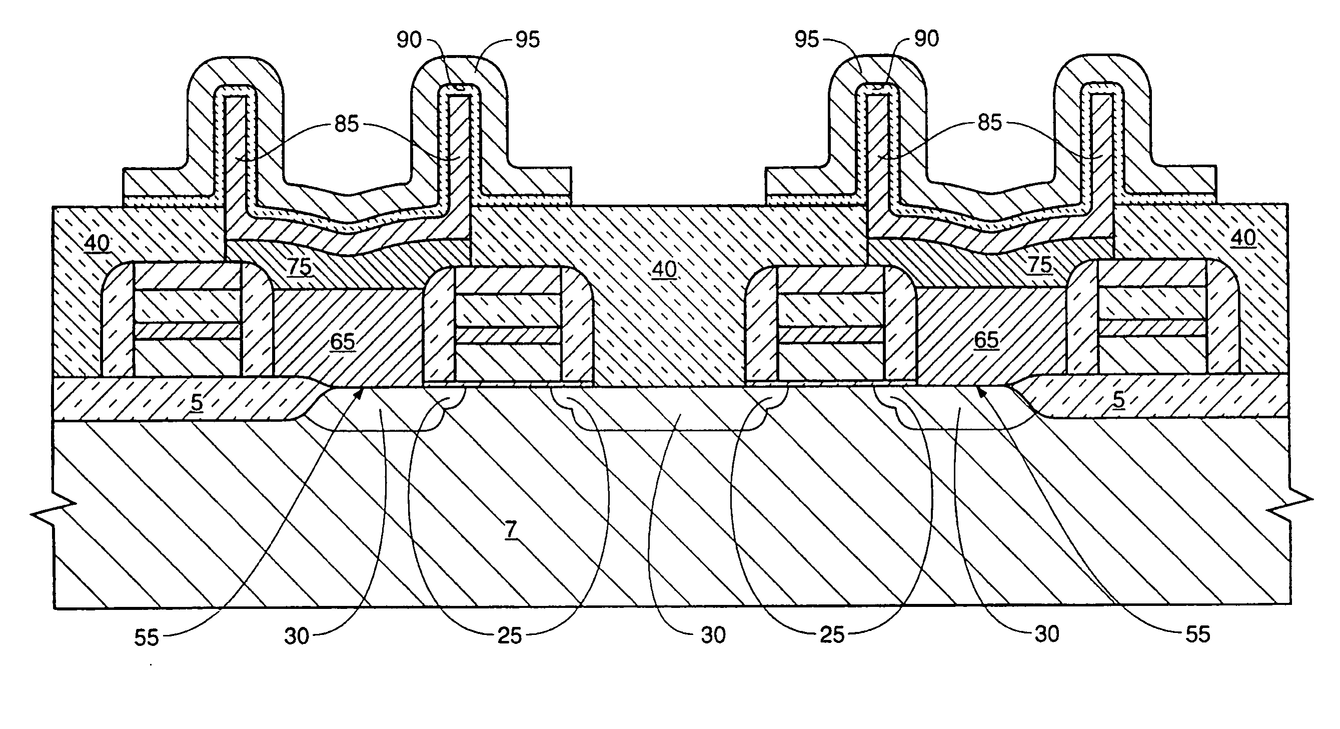
[0072] The method for fabricating the storage cell capacitor of the invention is shown pictorially in FIGS. 2-11.
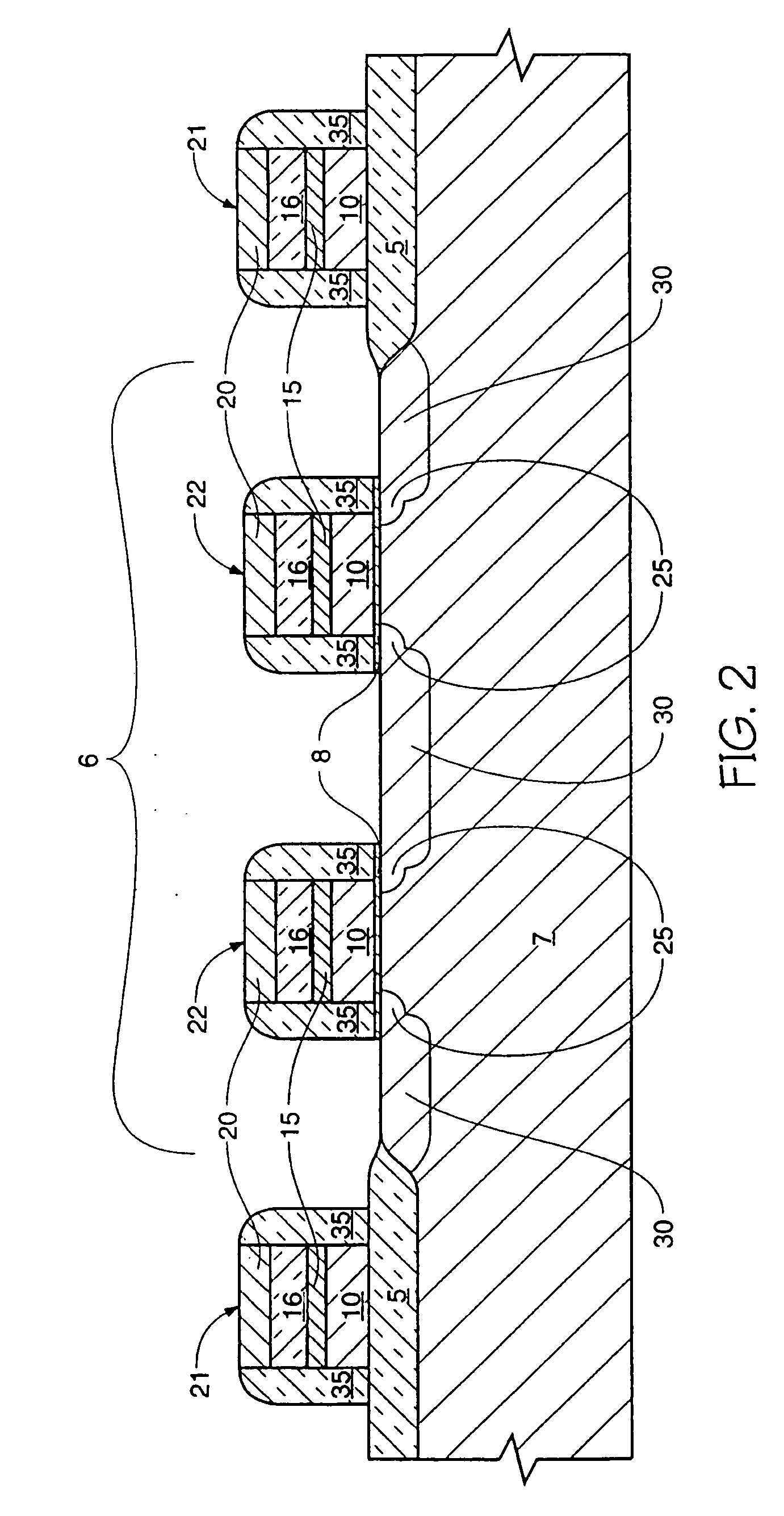
[0073] Referring to FIG. 2, a cross-sectional view of an in-process dynamic random access memory (DRAM) cell is shown following conventional local oxidation of silicon (LOCOS) or special LOCOS processing which creates substantially planar field oxide regions 5 (created using modified LOCOS or trench isolation processes) and future active areas 6 (those regions of the substrate not covered by field oxide) on a silicon substrate 7. The creation of the field oxide is preceded or followed by a thermally grown dielectric layer 8 of silicon oxide. The depicted cell is one of many cells that are fabricated simultaneously and comprise a memory array. Following the creation of the field oxide region 5 and dielectric layer 8 a first conductively doped polysilicon layer 10, a metal silicide layer (Wsix) 15, an oxide layer 16, and a thick nitride layer 20 are deposited. The thick ni...
PUM
| Property | Measurement | Unit |
|---|---|---|
| dielectric constant | aaaaa | aaaaa |
| dielectric constant | aaaaa | aaaaa |
| thickness | aaaaa | aaaaa |
Abstract
Description
Claims
Application Information