Supercharge Your Innovation With Domain-Expert AI Agents!

Light-emitting semiconductor device and method of fabrication

a technology of light-emitting semiconductor and manufacturing method, which is applied in the direction of semiconductor/solid-state device manufacturing, semiconductor devices, electrical apparatus, etc., can solve the problems of high absorption of gaas substrate, inconvenient forward voltage between the anode and the cathode of the light-emitting device, and unsatisfactory remedy. , to achieve the effect of improving the efficiency of light-emitting semiconductor devices

Inactive Publication Date: 2005-05-26
SANKEN ELECTRIC CO LTD
View PDF2 Cites 32 Cited by
  • Summary
  • Abstract
  • Description
  • Claims
  • Application Information

AI Technical Summary

Benefits of technology

The present invention aims to improve the efficiency of light-emitting semiconductor devices by improving the reflection of light from the semiconductor region to the reflective metal layer. The invention includes a semiconductor region with a first and second semiconductor layer, a transparent layer, and a reflective metal layer. The transparent layer is in ohmic contact with both semiconductor layers and reflects the light generated by the semiconductor region. The reflective metal layer makes ohmic contact with a greater surface area of the neighboring part, reducing the resistivity of the current path and enhancing the efficiency of the device. The thickness of the transparent layer is preferably between 10 nanometers and one micrometer. The invention also includes a baseplate for stable mechanical support and a contact layer to prevent light reflection. The technical effects of the invention include improved efficiency of light emission and reduced power loss.

Problems solved by technology

One of the problems encountered with this conventional light-emitting device is that the GaAs substrate is highly absorptive of the light in the wavelength range emitted by the active semiconductor layers.
This remedy proved unsatisfactory, however, as the active semiconductor layers and the transparent support substrate gave rise to electrical resistance at the interface therebetween.
This resistance made the forward voltage between the anode and cathode of the light emitting device inconveniently high.
The aluminum layer makes no satisfactory ohmic contact with the exposed surface of the active semiconductor layers.
However, this second recited prior art device also proved to have its own weaknesses.
One of these weaknesses arose in conjunction with the manufacturing process of the device, which involved several heat treatments.
Undesired reactions took place as a result of such heat treatments between the reflective metal layer, the Au—Ge—Ga alloy regions, and the neighboring part of the active semiconductor layers.
The result was a diminution of reflectivity at their interfaces.
High-efficiency light-emitting devices were therefore not obtainable with as high a yield as had been expected.
Another weakness concerned the isolated regions of Au—Ge—Ga alloy on the underside of the active semiconductor layers.
These isolated alloy regions made it difficult to fulfill both of the objectives of higher efficiency of light emission and the reduction of the forward voltage.
This reduction of efficiency came from less reflection of light from the active semiconductor layers by the aluminum layer because of the isolated regions of larger size interposed therebetween.

Method used


Image

  • Light-emitting semiconductor device and method of fabrication
  • Light-emitting semiconductor device and method of fabrication
  • Light-emitting semiconductor device and method of fabrication

Examples


embodiment

of FIG. 3

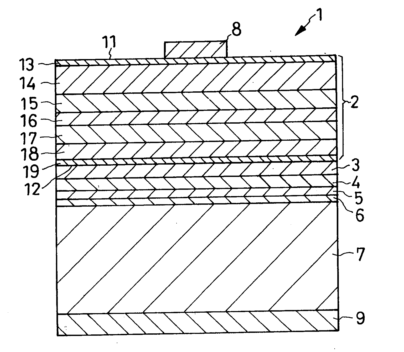
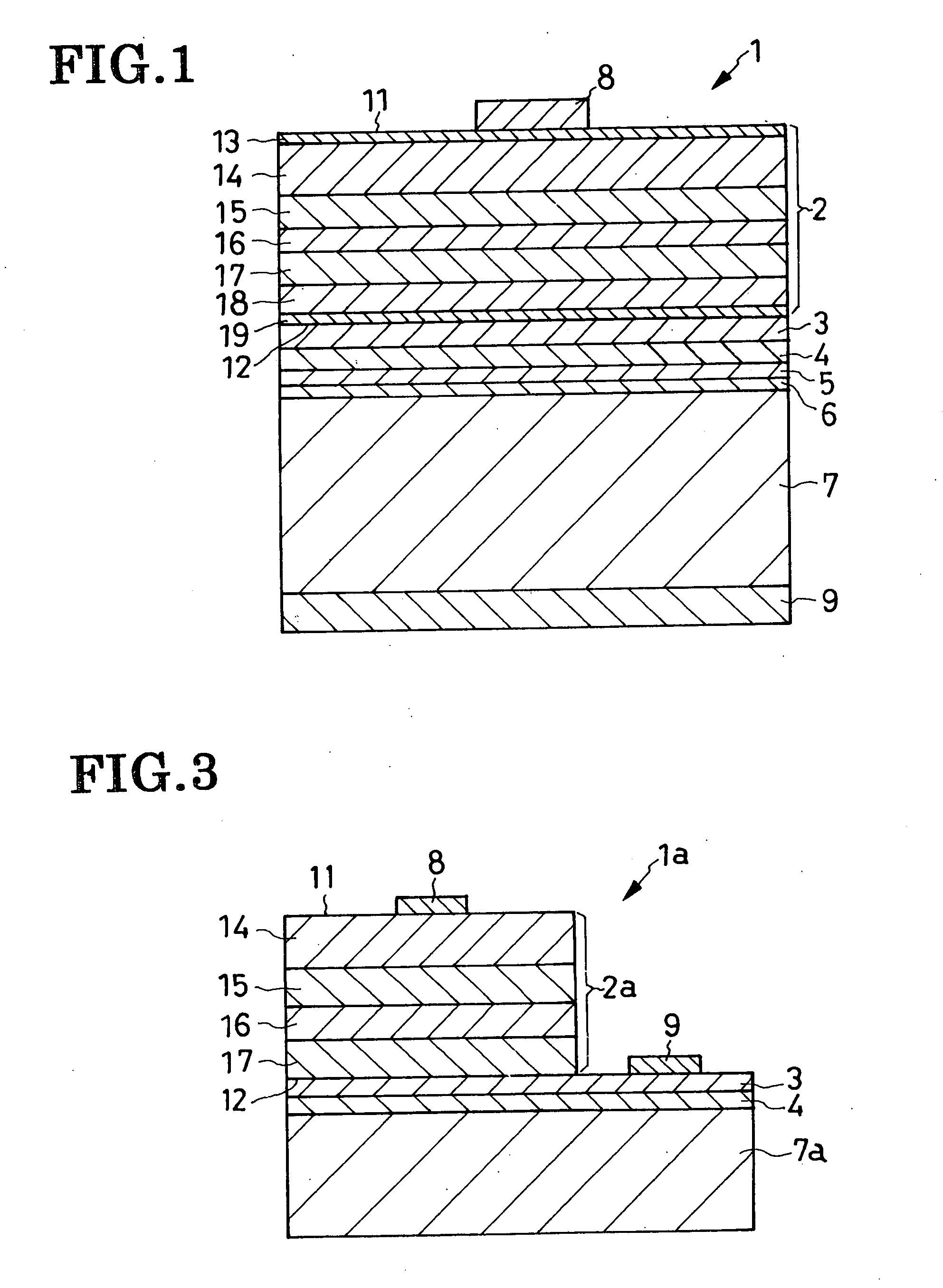
[0064]FIG. 3 illustrates another preferred form of LED 1a according to the invention, which differs from the FIG. 1 device in having a modified semiconductor region 2a, modified baseplate 7a, and modified positioning of the anode 9. The modified semiconductor region 2a is akin to its FIG. 1 counterpart 2 except for the absence of the first and third complementary layers 13 and 18 and contact layer 19. The cathode 8 is therefore mounted on the surface 11 of the complementary layer 14, which may be more aptly termed the current spreading layer in this alternate embodiment of the invention.

[0065] The modified baseplate 7a and the transparent layer 3 and reflective layer 4 thereon have portions projecting laterally beyond the overlying semiconductor region 2a. The anode is arranged on the ledge or ledges thus formed by the baseplate 7a and layers 3 and 4, making direct contact with the transparent layer 3. The reflective layer 4 is coupled directly to the baseplate 7a. The bas...


PUM


Abstract

A light emitting diode has a semiconductor region for production of light. The semiconductor region is a lamination of two complementary layers, an n-type semiconductor layer, an active layer, a p-type semiconductor layer, another complementary layer, and an ohmic contact layer, in that order from a first major surface of the semiconductor layer, from which the light is emitted, toward a second. A reflective metal layer covers the second major surface of the semiconductor region via a transparent layer for reflecting the light that has traveled through the transparent layer from the semiconductor region. The transparent layer serves to prevent the semiconductor region and the reflective layer from alloying by heat treatments during the manufacture of the LED.

Description

CROSS REFERNCE TO RELATED APPLICATIONS [0001] This application claims priority to Japanese Patent Application No.2003-392944, filed Nov. 21, 2003. BACKGROUND OF THE INVENTION [0002] This invention relates to a light-emitting semiconductor device, or light-emitting diode according to more common parlance, and more particularly to such devices having active layers made from chemical compounds such for example as aluminum gallium arsenide (AlGaAs), aluminum gallium indium phosphide (AlGaInP), and gallium nitride (GaN). The invention also concerns a method of making such light-emitting devices. [0003] Compound semiconductors containing AlGaInP, for instance, represent familiar materials of light-emitting semiconductor devices. An example of such device has a substrate of gallium arsenide (GaAs) on which there are laminated a plurality of active semiconductor layers composed primarily of AlGaInP. The active semiconductor layers for generating light include an n-type semiconductor layer, ...

Claims


Application Information

Patent Timeline
Patent Type & Authority Applications(United States)
IPC IPC(8): H01L29/24H01L33/00H01L33/46
CPCH01L21/42H01L33/46H01L33/0079H01L33/0093
Inventor TAKEDAMUROFUSHI, HITOSHI
Owner SANKEN ELECTRIC CO LTD
Features
  • R&D
  • Intellectual Property
  • Life Sciences
  • Materials
  • Tech Scout
  • Unparalleled Data Quality
  • Higher Quality Content
  • 60% Fewer Hallucinations
Learn More