Methods for producing and using catalytic substrates for carbon nanotube growth
a technology of carbon nanotubes and substrates, applied in the field of nanotechnology, can solve the problems of inherently disadvantageous techniques, atomic force microscopy is the size and shape of the scanning probe tip, and the cost of solid carbon vaporization via electric arc or laser apparatus is both costly and difficult to operate on commercial or industrial scales
- Summary
- Abstract
- Description
- Claims
- Application Information
AI Technical Summary
Benefits of technology
Problems solved by technology
Method used
Image
Examples
example 1
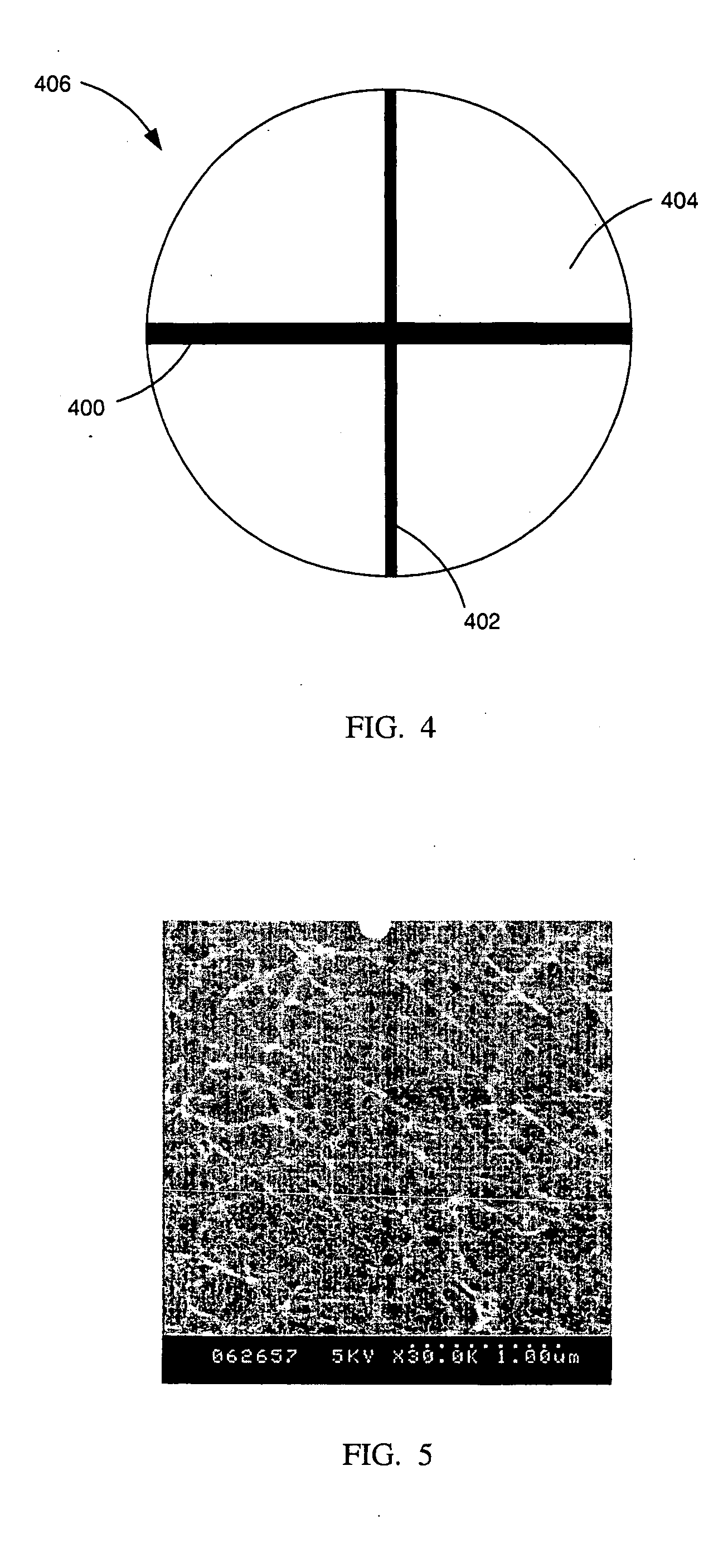
[0053]FIG. 4 is a schematic diagram showing a strip 400 of an Fe foil and a strip 402 of a Mo foil disposed on top of an Al sputtering target 404 with an exemplary diameter of 2.54 cm to form a co-sputtering target 406. In this example the strip 400 of the Fe foil has a width of about 1 mm and the strip 402 of the Mo foil has a width of about 0.5 mm. In one exemplary deposition run, DC sputtering of the co-sputtering target 406 deposited the precursor layer at a rate of 6 nm per minute. Hence, a 3 nm thick precursor layer can be obtained by sputtering for 30 seconds and a 20 nm thick precursor layer can be obtained by sputtering for about 3 minutes. The concentrations of Fe and Mo in the precursor layer are determined by the relative areas of the strips 400, 402 of the co-sputtering target 406.
[0054] After sputtering, the precursor layer can be annealed in air at a temperature in a range from about 400° C. to about 900° C. for a period of time ranging from about 5 to about 30 minut...
example 2
[0056] A 20 nm thick thin film of a Al / Fe / Mo precursor layer was prepared by co-sputtering Al, Fe, Mo in the ratio of 96.1:2.6:1.3 for 3 minutes in a DC sputtering system operating at 50 W power and under a vacuum of 5×10⁻³ mbar. The concentrations of Fe and Mo, 2.6% and 1.3% respectively, were achieved according to the relative areas of Fe and Mo strips 400, 402 in the co-sputtering target 406 of Example 1. The deposited precursor layer was then heated in air at 600° C. for 30 minutes to produce the catalyst material 100. CVD growth of nanotubes under the conditions described in Example 1 on the catalyst material 100 was performed to produce nanotubes as shown in the scanning electron microscope (SEM) micrograph of FIG. 5. This SEM micrograph shows a mat of uniformly distributed and interconnected nanotubes.
example 3
[0057] A patterned catalyst material 100 was prepared by a standard photolithography procedure including spin-coating a photoresist layer on the substrate 106, exposing the photoresist layer through a mask to establish a pattern, and developing the exposed photoresist layer to leave areas of the substrate 106 exposed and other areas covered with the photoresist layer. Next, the catalyst material 100 was deposited according to an embodiment of the invention described above. Finally, the remaining photoresist layer was removed with acetone.
[0058]FIG. 6 shows an AFM image of nanotubes grown from a catalyst material 100 produced from a patterned 20 nm thick Al / Fe / Mo precursor layer. It will be understood that only the right edge of the image in FIG. 6 shows an area in which the catalyst material 100 was patterned, while the remainder of the image shows an area that was protected by the photoresist layer during the deposition of the precursor layer. It can be seen that nanotubes 600 hav...
PUM
| Property | Measurement | Unit |
|---|---|---|
| Temperature | aaaaa | aaaaa |
| Temperature | aaaaa | aaaaa |
| Temperature | aaaaa | aaaaa |
Abstract
Description
Claims
Application Information


