

Method of manufacturing electro-optical device, electro-optical device, and electronic apparatus comprising the same
a manufacturing method and technology of electrooptical devices, applied in the direction of discharge tubes luminescnet screens, identification means, instruments, etc., can solve the problems of reducing manufacturing yield, uneven thickness, and insufficient etching, so as to reduce the appearance of spots or stain, reduce the effect of etching, and improve the control
- Summary
- Abstract
- Description
- Claims
- Application Information
AI Technical Summary
Benefits of technology
Problems solved by technology
Method used
Image

Examples
example 1
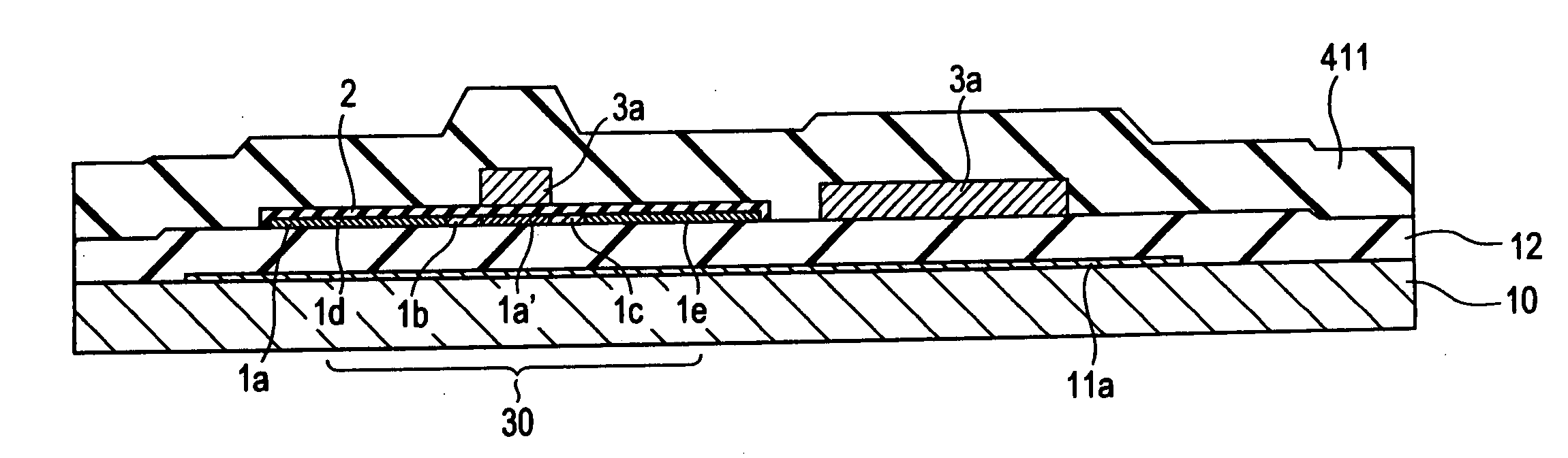
[0133] Similar to the above exemplary embodiment, an electro-optical device is manufactured. In that case, as shown in FIG. 10, a pattern 61 is formed on a quartz substrate, and a BPSG film 62 is formed over the entire surface of the quartz substrate to have a film thickness of 800 nm. The pattern 61 corresponds to the scanning line 3a in the exemplary embodiment, and the BPSG film 62 corresponds to the first interlayer insulating film 41 in the exemplary embodiment. Next, the substrate is heat-treated at 890° C., and the BPSG film 61 is subjected to planarizing treatment by reflow. After the planarizing treatment, the angle of inclination of a stepped portion of the BPSG film 62 caused by the pattern 61 is measured as a reflow angle θ.
[0134] The above processes are performed while the concentration of boron (B) of the BPSG film 62 is changed from 0.8 percent by weight to 5 percent by weight. In all the cases, the concentration of phosphorus (P) is 6 percent by weight.
[0135] The m...
example 2
[0137] Similar to Example 1, an electro-optical device is manufactured. However, when a BPSG film 62 is formed on a quartz substrate in which a pattern 61 is formed, in this Example, the concentration of boron of the BPSG film 62 is fixed to 3 percent by weight and the concentration of phosphorus (P) is fixed to 6 percent by weight. In addition, planarizing treatment is performed while the heating temperature (reflow temperature) is changed to 850° C., 900° C., and 950° C., and the reflow angle θ is measured in the respective cases.
[0138] The measurement results obtained in these cases are shown in FIG. 12. FIG. 12 illustrates a change of the reflow angle θ with respect to the reflow temperature of the BPSG film 62. It can be understood that, at a reflow temperature of about 850° C., the reflow angle θ is about 86°, and the height difference is still steep. However, it can be understood that, at a reflow temperature of 900° C., the reflow angle θ is 45° C., and the height differenc...
example 3
[0140] Next, a situation in which phosphorus and boron precipitates is shown in Table 1. When a BPSG film in which the amount of phosphorus and boron change is formed, is a situation in which phosphorus and boron precipitates can be investigated by visual inspection. In addition, the flow rate of ozone in forming a BPSG film is kept constant (80 slm) in all samples.
TABLE 1PBP + BDays of Pre-(Percent by(Percent by(Percent bycipitation (anyMassweight)weight)weight)of P and B)Productivity549>7 days⊚459 7 days◯55102 to 3 daysΔ5611×6511×
[0141] As shown in Table 1, in a BPSG film whose total percent by weight of phosphorus and boron is 11 percent by weight, it is confirmed that phosphorus or boron precipitates in a day after the film is formed. Also, the present inventors have confirmed that, as the total percent by weight of phosphorus and boron decreases, the period until phosphorus or boron precipitates is prolonged. Further, in a condition that the total percent by weight of phospho...
PUM
 Abstract
Description
Claims
Application Information