
Nanoparticle deposition process

a technology of nanoparticles and deposition processes, applied in the direction of nanostructure manufacturing, transportation and packaging, coatings, etc., can solve the problems of high cost of vacuum deposition and photolithography, and is not suitable for manufacturing low-cost large-area electronics

Inactive Publication Date: 2005-06-16
XEROX CORP
View PDF17 Cites 98 Cited by
  • Summary
  • Abstract
  • Description
  • Claims
  • Application Information

AI Technical Summary

Problems solved by technology

However, vacuum deposition and photolithography are costly techniques.
They are not suitable for use in manufacturing low-cost large-area electronics, particularly plastic electronics.

Method used

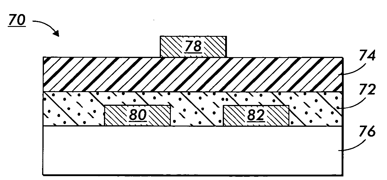
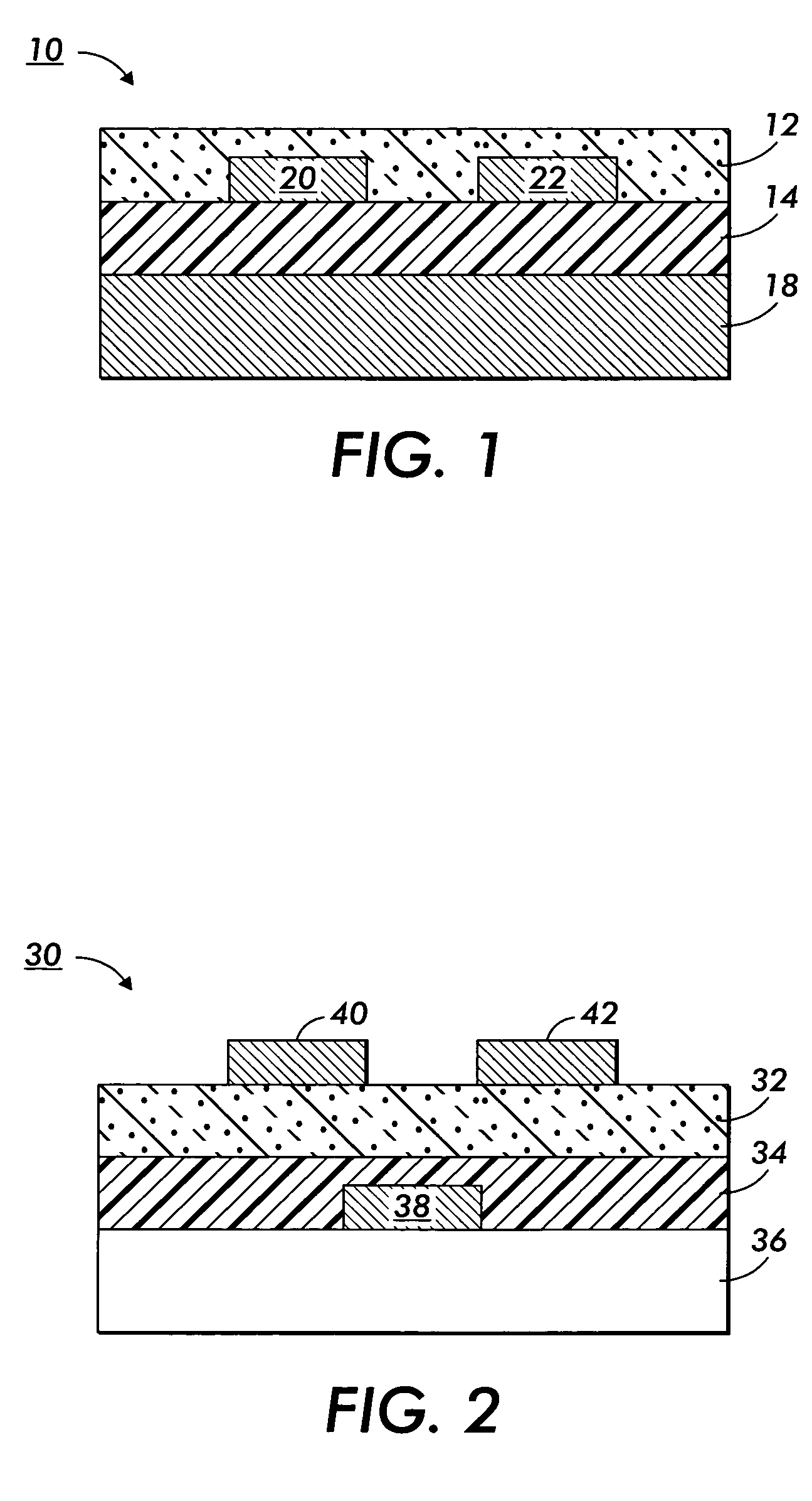
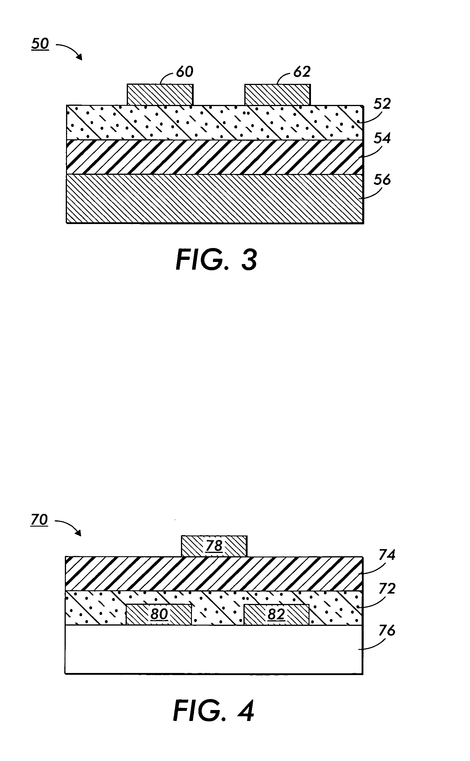

Image

  • Nanoparticle deposition process
  • Nanoparticle deposition process
  • Nanoparticle deposition process

Examples


example 1

Preparation of Gold Nanoparticles with an Alkanethiol Stabilizer

[0074] To a tetraoctylammonium bromide (2.19 g, 4 mmol) solution in toluene (80 mL) in a 500 mL flask was added hydrogen tetrachloroaurate (III) trihydrate (0.394 g, 1 mmol) solution in water (100 mL) with rapid stirring (under argon). After two minutes, 1-octanethiol (0.439 g, 3 mmol) in toluene (30 mL) was added to the flask and stirred vigorously for 10 min at room temperature until the solution became colorless. Then the solution was cooled to 0° C. by an ice-water bath. A freshly prepared sodium borohydride (0.378 g, 10 mmol) solution in water (100 mL) was added to the vigorously stirred solution over 30 seconds. The reaction mixture was allowed to warm to room temperature and the rapid stirring was continued for 3 h. The organic phase was separated and concentrated to 5 mL by evaporation of the solvent (the bath temperature is <40° C.). The concentrated solution was added drop-wise to 200 mL rapidly stirring meth...

example 2

Preparation of Silver Nanoparticles with an Alkanethiol Stabilizer

[0075] Silver nanoparticles stabilized with n-octanethiol were prepared according to the procedure as described in Example 1 using silver nitrate (0.17 g, 1 mmol). A dark brown solid (0.18 g) was obtained after work-up.

example 3

Preparation of Gold Nanoparticles with Organophosphine Stabilizer

[0076] To a tetraoctylammonium bromide (1.60 g, 2.93 mmol) solution in toluene (50 mL) in a 500 mL flask was added hydrogen tetrachloroaurate (III) trihydrate (1.00 g, 2.54 mmol) solution in water (65 mL) with rapid stirring (under argon). After two minutes, triphenylphosphine (2.32 g, 8.85 mmol) was added to the flask and stirred vigorously for 10 min at room temperature. Then the solution was cooled to 0 degree C. by an ice-water bath. A freshly prepared sodium borohydride (1.41 g, 37.3 mmol) solution in water (10 mL) was added to the vigorously stirred solution over 30 seconds. The reaction mixture was allowed to warm to room temperature and the rapid stirring was continued for 3 h. The organic phase was washed with water 3 times, separated, dried over anhydrous magnesium sulfate, and filtered. The solvent was removed by evaporation (the bath temperature is <40° C.) to give a black solid. The solid was washed with ...


PUM

PropertyMeasurementUnit
particle sizeaaaaaaaaaa
conductivityaaaaaaaaaa

Abstract

A process including: (a) solution depositing a composition composed of a liquid and a plurality of metal nanoparticles with a stabilizer on a substrate to result in a deposited composition; and (b) heating the deposited composition to cause the metal nanoparticles to form an electrically conductive layer of an electronic device, wherein one or more of the liquid, the stabilizer, and a decomposed stabilizer is optionally part of the electrically conductive layer but if present is in a residual amount.

Description

BACKGROUND OF THE INVENTION [0001] The proper deposition and patterning of electrically conductive materials as for instance electrodes and interconnects are important in circuit fabrication for electronic devices. Electrodes of electronic devices such as thin film transistors can be fabricated, for example, by vacuum deposition of a metal through a shadow mask, or by vacuum deposition of a metal and subsequent patterning with photolithography technique. However, vacuum deposition and photolithography are costly techniques. They are not suitable for use in manufacturing low-cost large-area electronics, particularly plastic electronics. Manufacturing cost can be significantly reduced if the electrodes and interconnects could be directly deposited and patterned by solution depositing. In addition, although organic electrically conductive materials such as polystyrene sulfonate-doped poly(3,4-ethylenedioxythiophene) (“PSS-PEDOT”) are solution processable, metal is preferred over organi...

Claims


Application Information

Patent Timeline
Patent Type & Authority Applications(United States)
IPC IPC(8): B22F1/0545B82B3/00H01L21/28H01L21/288H01L21/336H01L21/44H01L23/532H01L29/786H10K99/00
CPCB22F1/0022Y10T428/25B22F2999/00B82Y30/00H01L21/288H01L23/53242H01L51/0004H01L51/0021H01L51/0022H01L51/0036H01L51/0545H01L51/055H01L51/102H01L2924/12044B22F7/04Y10S977/936H01L2924/0002B22F1/0074B22F1/0085H01L2924/00B22F1/0545H10K71/13H10K71/611H10K71/60H10K85/113H10K10/481H10K10/466H10K10/82B22F1/142B22F1/107
Inventor WU, YILIANGLI, YUNINGONG, BENG S.
Owner XEROX CORP
Learn More