Optical receiver circuit

a receiver circuit and optical receiver technology, applied in the direction of amplifiers with min 3 electrodes or 2 pn junctions, electromagnetic transmission, instruments, etc., can solve the problem of negligible error of finite extinction rate in most systems, and achieve the effect of low area requirement and current consumption

Active Publication Date: 2005-06-23
AVAGO TECH INT SALES PTE LTD
View PDF1 Cites 33 Cited by
  • Summary
  • Abstract
  • Description
  • Claims
  • Application Information

AI Technical Summary

Benefits of technology

[0006] The present invention provides an optical receiver circuit having signal detection, in which the receiver circuit manages with as few additional components as possible, a

Problems solved by technology

However, the error of the finite extinction rate is negligible in most systems on account of the minimum requirement

Method used


Image

  • Optical receiver circuit
  • Optical receiver circuit

Examples


Embodiment Construction

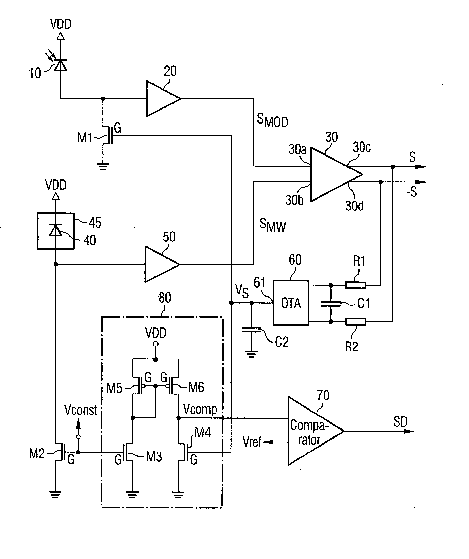
[0025] The receiver circuit has a first optoelectronic transducer 10 in the form of a photodiode, which converts an optical information signal into an electrical signal. The electrical signal is amplified in an input amplifier or preamplifier 20 and supplied to one input 30a of a postamplifier 30, which is a differential amplifier. The preamplifier 20 is preferably a transimpedance amplifier comprising a voltage amplifier and a negative feedback resistor (not illustrated in any more detail).

[0026] At the input of the preamplifier 20, a constant current of a regulatable current source, which is provided by a field effect transistor M1, is superposed on the essentially rectangular-waveform output signal of the photodiode 10. The current source M1 is regulated via the gate voltage present at the transistor M1. Instead of a field effect transistor, a bipolar transistor may, however, in principle also be used at this point and even otherwise in the circuit.

[0027] The current source M1 ...


PUM


Abstract

Optical receiver circuit having a first, illuminable reception device for converting an optical signal into an analog electrical signal; a first preamplifier for amplifying the output signal of the first reception device; a postamplifier having a first input and a second input, the first input being supplied with the signal of the first reception device (said signal having been amplified in the first preamplifier) and the second input being supplied with a reference signal; an offset compensation circuit, which regulates the difference between the mean value of the electrical signal at the first input of the postamplifier and the reference signal at the second input of the postamplifier to a constant value; and having a signal detection device, which detects a control signal of the offset compensation circuit and carries out signal detection in a manner dependent on this signal. The invention provides signal detection in an optical receiver circuit, which manages with few additional components.

Description

RELATED APPLICATION [0001] The present application claims priority of U.S. Patent Application Ser. No. 60 / 531,345 filed by Harald Doppke, Detlev Theil, Torsten Harms and Stefan van Waasen on Dec. 19, 2003.FIELD OF THE INVENTION [0002] The invention relates to an optical receiver circuit as used, in particular, to detect optical signals in digital optical receivers. BACKGROUND OF THE INVENTION [0003] For the reception and for the regeneration of optical signals after they have passed through a transmission system, digital optical receivers are known which comprise an analog input part, in which the optical signal is converted into an analog electrical signal, and a digital signal processing part, in which the analog signal is regenerated into a digital data signal having a normalized amplitude and clock information. In the analog part, the optical signal received is converted into a photocurrent by means of a photodiode and amplified in a preamplifier. [0004] It is known practice, in...

Claims


Application Information

Patent Timeline
IPC IPC(8): H04B10/158
CPCH04B10/6933
Inventor DOPPKE, HARALDTHEIL, DETLEVHARMS, TORSTENVAN WAASEN, STEFAN
Owner AVAGO TECH INT SALES PTE LTD
Why Eureka
Try Eureka