Image sensor for reduced dark current

Active Publication Date: 2005-06-23
APTINA IMAGING CORP
View PDF2 Cites 72 Cited by
  • Summary
  • Abstract
  • Description
  • Claims
  • Application Information

AI Technical Summary

Benefits of technology

[0008] The invention provides a method and structure for reducing dark current in an image sensor by preventing unwanted electrons from being c

Problems solved by technology

Another problem often associated with photodiodes is that of blooming.
Blooming is undes

Method used


Image

  • Image sensor for reduced dark current
  • Image sensor for reduced dark current
  • Image sensor for reduced dark current

Examples


first embodiment

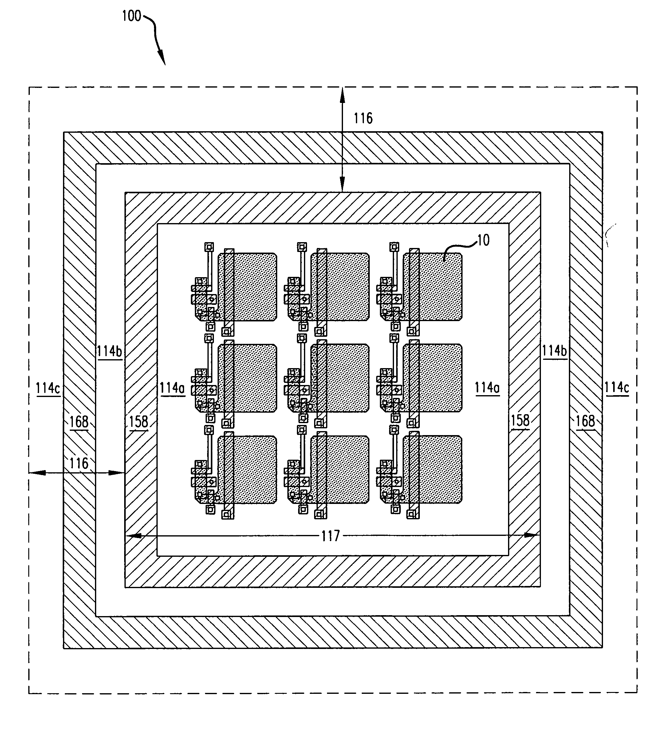
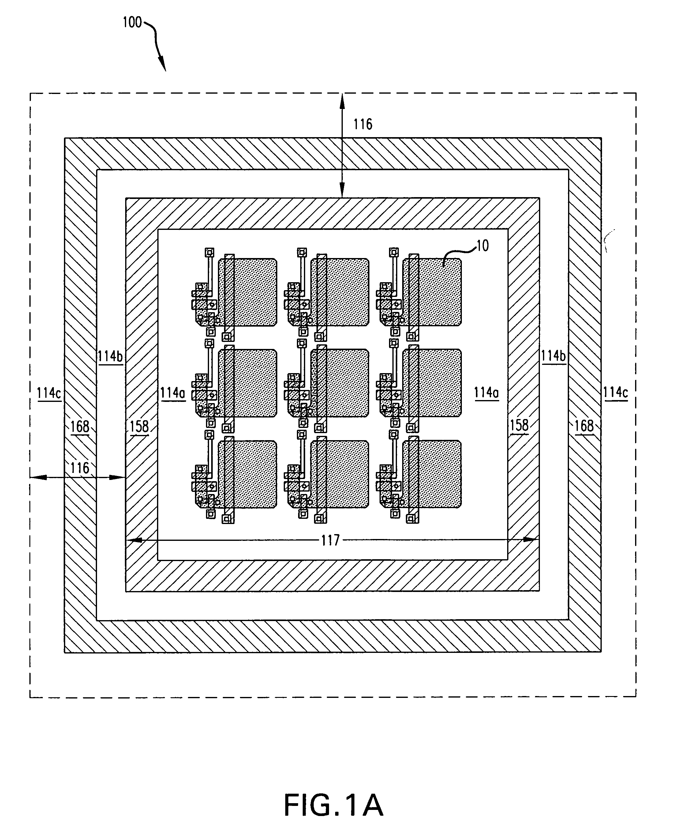
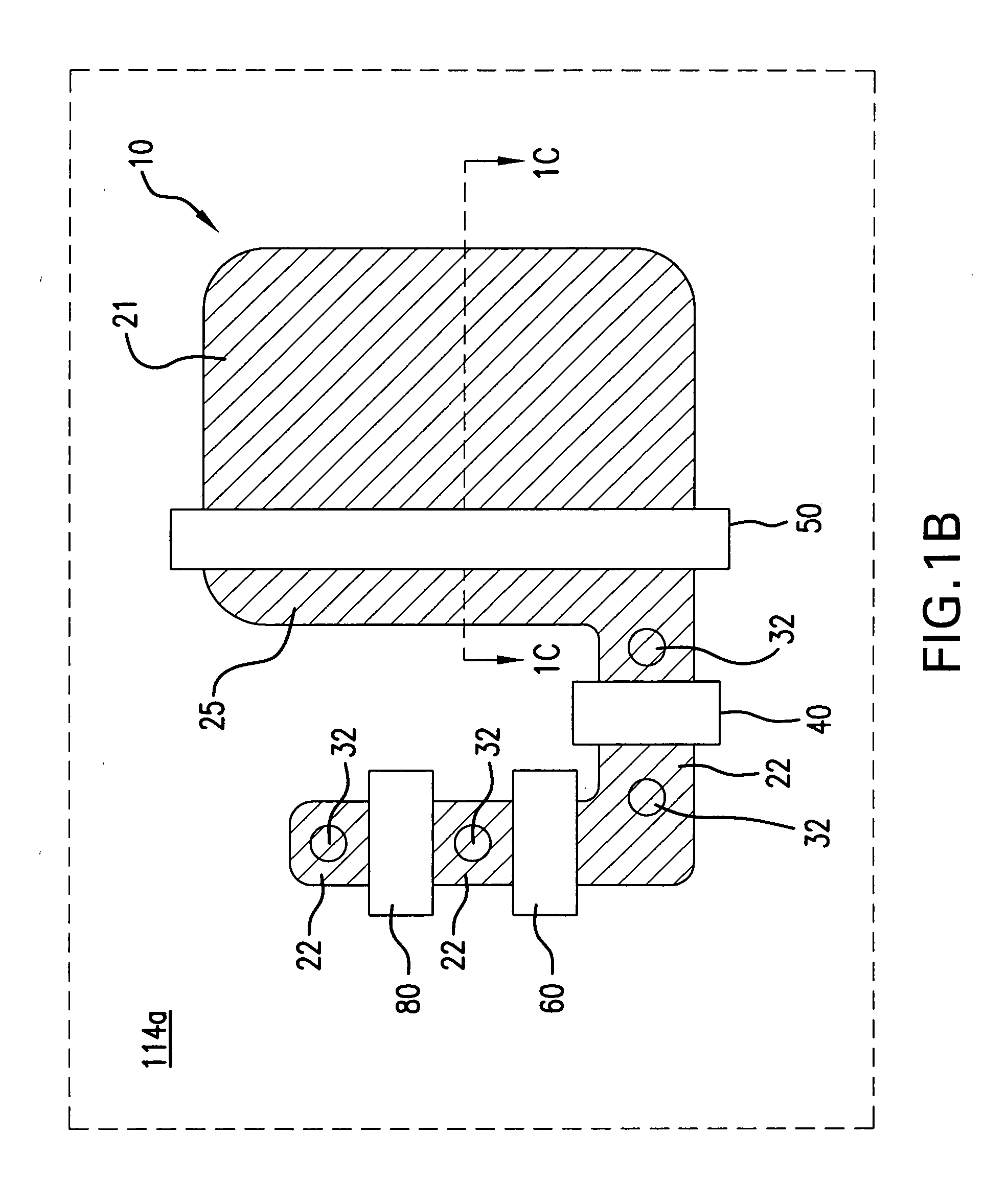
[0049] The CMOS image sensor in accordance with the first embodiment may be fabricated using several fabrication processes. In a preferred embodiment of the fabrication process, depicted in FIGS. 12-15, the field oxide regions 114 are formed first, i.e., before the n-type region 166, and n-type sidewall 168 are formed. Referring now to FIG. 12, a first conductivity type implant, for example p-type, is provided into a substrate 112. Next, field oxide regions 114a, 114b, and 114c are formed in substrate 112. Referring now to FIG. 13, a deep n-type region 166 is formed in substrate 112 above p-type substrate area 112a and below p-type substrate area 112b. Next, as depicted in FIG. 14, an n-type sidewall 168 is formed. The n-type sidewall 168 and n-type region 166 form an n-type region isolation structure which separates the pixel array region 117 from the peripheral circuit region 116. Referring now to FIG. 15, one or more p-well implants are performed into second p-type substrate area...

second embodiment

[0058] Referring now to FIG. 6, which illustrates a CMOS image sensor fragment in accordance with the invention, indicated generally by reference numeral 200. Such comprises a p-type epitaxial or layer 212 formed over an n-type silicon substrate 210. It is also possible to implant the wafer with a p-type dopant and create p-type layer 212. The substrate includes a pixel array substrate region 217 and a peripheral circuit region 216. Field oxide regions 214 are provided in association with the peripheral substrate region 216 and pixel array substrate region 217. Although conductivity types are denoted in the description, for example, the substrate 210 is described as n-type and the epitaxial layer 212 is described as being p-type, these may be reversed and the invention is not limited to the arrangement of conductivity types as shown and described.

[0059] A peripheral n-type sidewall 268 is formed to extend through the epitaxial layer 212, and electrically contact the n-type substrate...


PUM


Abstract

A method and structure for reducing dark current in an image sensor includes preventing unwanted electrons from being collected in the photosensitive region of the image sensor. In one embodiment, dark current is reduced by providing a deep n-type region having an n-type peripheral sidewall formed in a p-type substrate region underlying a pixel array region to separate the pixel array region from a peripheral circuitry region of the image sensor. The method and structure also provide improved protection from blooming.

Description

FIELD OF THE INVENTION [0001] The invention relates to improved semiconductor imaging devices and, in particular, to CMOS image sensors having reduced dark current. BACKGROUND OF THE INVENTION [0002] In silicon integrated circuit (IC) fabrication, it is often necessary to isolate devices that are formed in a single substrate from one another. The individual devices or circuit components subsequently are connected to other circuit elements to create a specific circuit configuration. [0003] A CMOS image sensor circuit includes a focal plane array of pixels, each one of the pixels includes a photo-conversion device, e.g., a photogate, photoconductor, or photodiode having an associated charge accumulation region within a substrate for accumulating photo-generated charge. Each pixel may include a transistor for transferring charge from the charge accumulation region to a diffusion node and a transistor for resetting the diffusion node to a predetermined charge level prior to charge trans...

Claims


Application Information

Patent Timeline
IPC IPC(8): H01L21/82H01L27/10H01L27/146H01L27/148
CPCH01L27/1463H01L27/14843H01L27/14654
Inventor RHODES, HOWARD E.COLE, STEVE
Owner APTINA IMAGING CORP
Why Eureka
Try Eureka