Method for manufacturing semiconductor device

a semiconductor and manufacturing technology, applied in the direction of capacitors, presses, textiles and paper, etc., can solve the problems of insufficient characteristic, oxygen deficit not made up, and inability to obtain sufficient characteristic, etc., to achieve high efficiency and recover the effect of deterioration of ferroelectric films

Inactive Publication Date: 2005-06-23
FUJITSU SEMICON LTD
View PDF21 Cites 25 Cited by
  • Summary
  • Abstract
  • Description
  • Claims
  • Application Information

AI Technical Summary

Benefits of technology

[0037] An object of the present invention is to provide a method for manufacturing a semiconductor

Problems solved by technology

Therefore, the sufficient characteristic can not be obtained.
However, the supply of oxygen from an exposed part (a side surface) of the PZT film is also interrupted, as a result, an oxygen deficit is not made up for.
Therefore, the sufficient characteristic can not be obtained.
Especially, in CVD method in which a wafer often suffered from heat, the deterioration of the ferroelectric film is conspicuous.
However, as a microfabrication art is progressed, a side wall of the capacitor becomes steep, so that a sufficient coverage can not be obtained by the sputtering process.
However, in the case of employing the CVD method as described above, the ferroelectric film is easy to deteriorate.
Thus, the moisture makes the ferroelectric

Method used


Image

  • Method for manufacturing semiconductor device
  • Method for manufacturing semiconductor device
  • Method for manufacturing semiconductor device

Examples


first embodiment

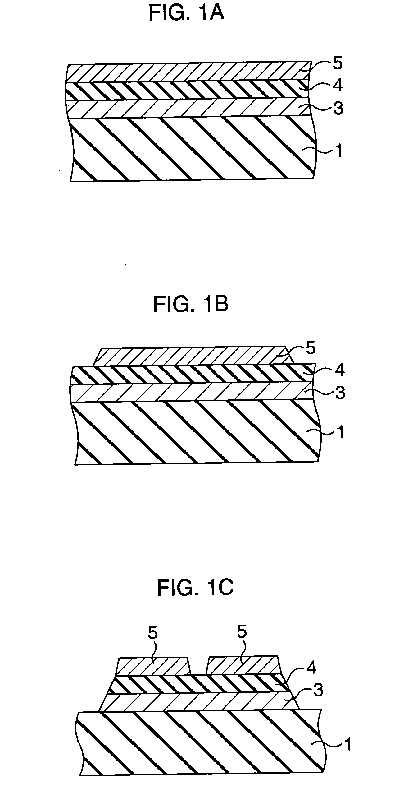
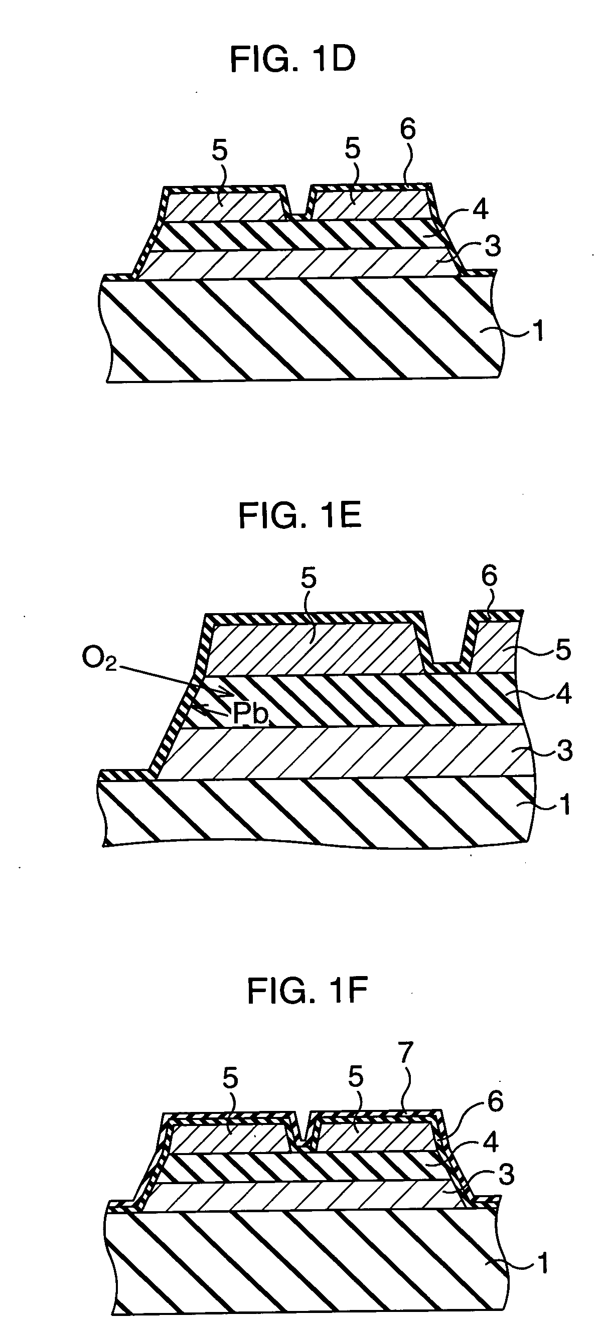
[0054] Hereinafter, some embodiments of the present invention will specifically described with reference to the accompanying drawings. FIG. 1A to FIG. 1F are sectional views showing a method for manufacturing a ferroelectric memory (a semiconductor device) having a ferroelectric capacitor according to the present invention. FIG. 2A and FIG. 2B are sectional views showing a configuration of a memory cell of the ferroelectric memory. FIG. 3 is a layout illustrating a relation between electrodes. FIG. 2A and FIG. 2B are sectional views taken along the I-I line, II-II line in FIG. 3 respectively.

[0055] In the present embodiment, as a memory cell, a ferroelectric memory in which planar 1T1C (1 transistor-1 capacitor)-type ferroelectric memory cells are arranged in an array is fabricated. In the following description, a direction in which a word line extends is called a row direction, and a direction orthogonal to a word line is called a column direction.

[0056] First, a field effect tran...

second embodiment

[0089] as described above, a good deal of damage is generated on the PZT film 4 on forming the interlayer insulating film 53, however, oxygen is supplied to the PZT film 4 via the vicinity of the interface between the upper electrode film 5 and the PZT film 4 by the oxygen anneal before the formation of the thick interlayer insulating film 54, so that damages such as the oxygen deficit of the PZT film 4 can be recovered easily and surely.

[0090] In other words, in the second embodiment, after the comparatively thin interlayer insulating film 53 is formed, the oxygen anneal is conducted before the thick interlayer insulating film 54 is formed, so that damages of PZT film 4 can be recovered with high efficiency. Besides, in the present embodiment, from the standpoint that the thickness of the alumina film is thinner than the other parts, at the vicinity of the interface between the upper electrode and the capacity insulating film, the oxygen deficit can be easily made up for. The reas...

third embodiment

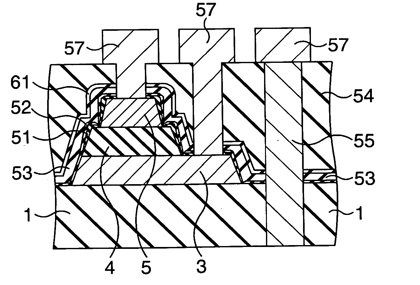
[0102] as described above, the Al2O3 film 61 is formed before the interlayer insulating film 54 is formed, so that the diffusion of hydrogen and / or moisture to the ferroelectric capacitor on forming the interlayer insulating film 54 is suppressed more efficiently. As the result, a high value related to a capacitor characteristic such as an imprint characteristic can be obtained.

[0103] Hereinafter, a result of an experiment related to the imprint characteristic, according to the second and third embodiments, actually made by the present inventors will be explained. FIG. 9 is a graph showing imprint characteristics of the second and third embodiments compared with the imprint characteristic of prior art (conventional example). A vertical axis in left side of FIG. 9 [Q3(88)@3V: bar graph] shows a polarization amount at the time when 88 hours has passed since data was written in 3V. A vertical axis in right side of FIG. 9 (Q3 rate: sequential graph) shows the changes of the polarizatio...


PUM


Abstract

An Al2O3 film for covering a ferroelectric capacitor is formed by a sputtering process. The thickness of the Al2O3 film is preferably optimized according to amount of remanent polarization and fatigue tolerance required for the ferroelectric capacitor, for example, 10 nm to 100 nm. Next, oxygen is supplied to a PZT film via the Al203 film by executing a heat treatment in an oxygen atmosphere. As a result, an oxygen deficit in the PZT film is made up for. At this time, evaporation of Pb in the PZT film is suppressed because of the Al2O3 film, and deterioration of the fatigue tolerance responsive to decrease of Pb amount is suppressed. Subsequently, another Al2O3 film is formed as a second protective film by the sputtering process for opposing the deterioration factor in later process. The thickness of the Al2O3 film is preferably the thickness which sufficiently protects the ferroelectric capacitor from the deterioration factor in later wiring process.

Description

CROSS-REFERENCE TO RELATED APPLICATIONS [0001] This application is based upon and claims the benefit of priority from the prior Japanese Patent Application No. 2003-425786, filed on Dec. 22, 2003, the entire contents of which are incorporated herein by reference. BACKGROUND OF THE INVENTION [0002] 1. Field of the Invention [0003] The present invention relates to a method for manufacturing a semiconductor device suitable for a ferroelectric memory. [0004] 2. Description of the Related Art [0005] In the process of forming a ferroelectric capacitor used for a ferroelectric memory and the like, an anneal is required for recovering damages of a ferroelectric film. [0006]FIG. 10A to FIG. 10C are sectional views showing a first example (a first prior art) of the conventional method for manufacturing a semiconductor device having a ferroelectric capacitor in order of processes. In the first prior art, as shown in FIG. 10A, a ferroelectric capacitor composing of a lower electrode 103, a PZT ...

Claims


Application Information

Patent Timeline
IPC IPC(8): H01L21/00H01L21/02H01L21/326H01L27/105H01L21/479H01L21/82H01L21/8246
CPCH01L28/57H01L27/11507H10B53/30D21J3/00D21J7/00B30B15/0082
Inventor OKITA, YOICHIWATANABE, JUNICHISASHIDA, NAOYA
Owner FUJITSU SEMICON LTD
Why Eureka
Try Eureka