Semiconductor light-emitting device and process for producing the same

Inactive Publication Date: 2005-07-07
SONY CORP
View PDF11 Cites 8 Cited by
  • Summary
  • Abstract
  • Description
  • Claims
  • Application Information

AI Technical Summary

Benefits of technology

[0022] The present invention relates to semiconductor light-emitting devices and methods of producing same. The light-emitting devices of the present invention include

Problems solved by technology

A disadvantage of growing gallium nitride on a sapphire substrate is that dislocations may densely exist in the crystals due to lattice mismatch between them.
Unfortunately, dry etching inevitably damages the crystal face.
Therefore, it has never been used for electronic devices and light-emitting devices, and is merely used as an underlying layer of crystal structure for further selective growth.
A disadvantage of this structure is that the horizontally spread electrodes make for extremely difficult and time-consuming work because one must separate miniature chips without cutting the horizontally spread electrodes.
Moreover, the sapphire substrate and nitride (such as GaN) are so hard that they are difficult to cut and require a cutting allowance of about 20 μm (i.e., micrometers), thereby making it even more difficult to cut the miniature chips.
Additionally, a problem with a light-emitting device in which the principal plane of the substrate is a C+-plane and the active layer of gallium nitride is formed parallel to the principal plane of the substrate is that there is only one bond from gallium atoms to nitrogen atoms in the C+-plane and hence, nitrogen atoms easily dissociate from the crystal face of the C+-plane, thereby making it difficult for the effective V/III ratio to be large, which in turn prevents improvement in performance of crystals constituting the light-emitting device.
However, it presents difficulties in forming the n-electrode accurately because large production steps occur in its vicinity after the mask layer has been removed.
A disad

Method used


Image

  • Semiconductor light-emitting device and process for producing the same
  • Semiconductor light-emitting device and process for producing the same
  • Semiconductor light-emitting device and process for producing the same

Examples


Example

Example 1

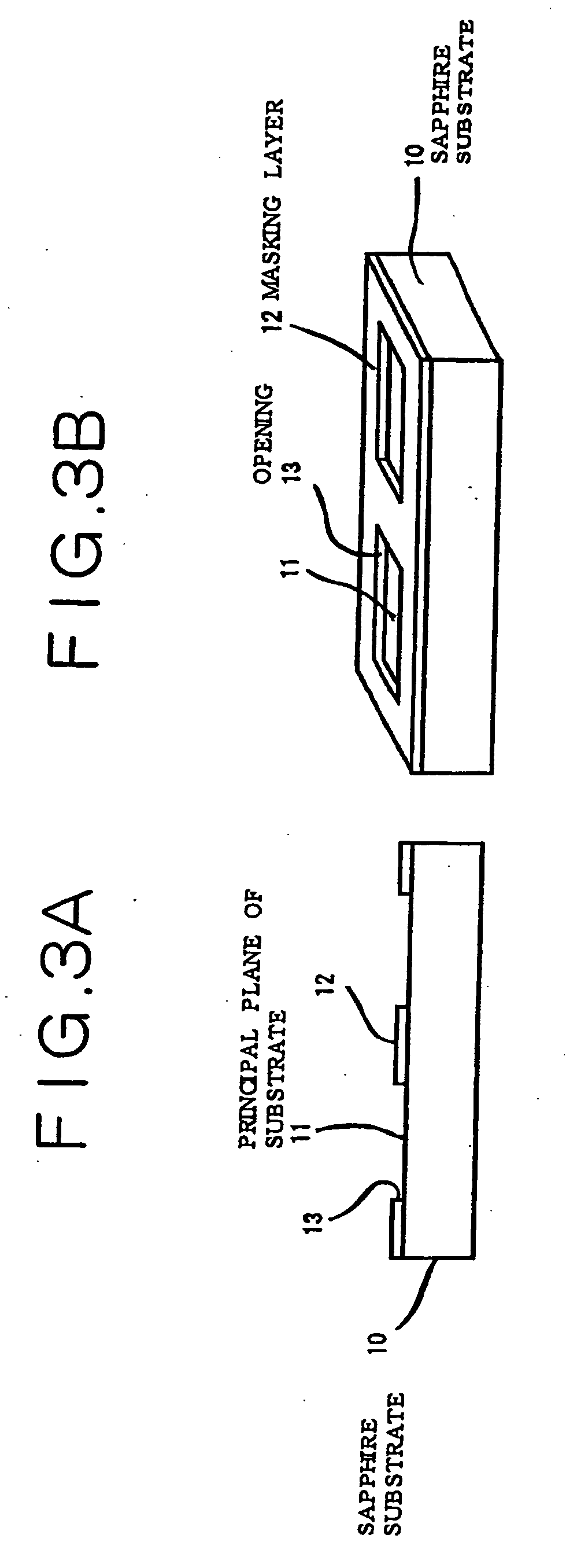
[0272] This example demonstrates a semiconductor light-emitting device which has a crystal layer formed by selective growth directly on a sapphire substrate. Additionally, the crystal layer includes a crystal surface having the S-plane as the slant crystal plane (i.e. the crystal surface plane that diagonally intersects the principal plane of the substrate). Its production process and structure will be described with reference to FIGS. 3A to 9.

[0273] The sapphire substrate 10 has the C+-plane as its principal plane 11 (i.e. the substrate surface plane). On the entire surface of the sapphire substrate 10 is formed the masking layer 12 (about 100 nm to about 500 nm thick) of SiO2 or SiN. In the masking layer 12 is formed the opening 13 (about 100 μm) by photolithography and etching with hydrofluoric acid based compound (see FIGS. 3A and 3B). In this Example, the opening 13 is in an approximately rectangular shape, but the size of the opening may be changed according to the ...

Example

Example 2

[0281] This example demonstrates a semiconductor light-emitting device which has a crystal layer (having the S-plane slanting to the principal plane of the substrate) formed on a crystal seed layer isolated from a sapphire substrate. Its production process and structure will be described with reference to FIGS. 10A to 17B.

[0282] On the sapphire substrate 30, whose principal plane is the C+-plane, is formed a buffer layer of AlN or GaN at a low temperature of about 500° C. Then, with the temperature raised to about 1000° C., the silicon-doped GaN layer 31 is formed. On the entire surface of the silicon-doped GaN layer 31 is formed a masking layer (about 100 nm to about 500 nm thick) of SiO2 or SiN. The masking layer is removed by photolithography and etching with hydrofluoric acid based compound except for the round masking part 32 (about 10 μm in diameter), as shown in FIGS. 10A and 1B. Etching is performed so that the principal plane of the sapphire substrate 30 is expos...

Example

Example 3

[0290] This example demonstrates a semiconductor light-emitting device in which the crystal layer in the shape of hexagonal pyramid (which has the S-plane slanting to the principal plane of the substrate) is formed within the window region for the selective mask. Its production process and structure will be described with reference to FIGS. 18A to 23.

[0291] On the sapphire substrate 40, whose principal plane is the C+-plane, is formed a buffer layer of AlN or GaN at a low temperature of about 5000° C. Then, with the temperature raised to about 1000° C., the silicon-doped GaN layer 41 is formed. On the entire surface of the silicon-doped GaN layer 41 is formed the masking layer 42 (about 100 nm to about 500 nm thick) of SiO2 or SiN. In the masking layer 42 is formed a round opening (about 10 μm in diameter) as the window region 43 by photolithography and etching with hydrofluoric acid based compound, as shown in FIGS. 18A and 18B. The size of the opening varies depending o...


PUM


Abstract

Semiconductor light-emitting devices are provided. The semiconductor light-emitting devices include a substrate and a crystal layer selectively grown thereon at least a portion of the crystal layer is oriented along a plane that slants to or diagonally intersect a principal plane of orientation associated with the substrate thereby for example, enhancing crystal properties, preventing threading dislocations, and facilitating device miniaturization and separation during manufacturing and use thereof.

Description

CROSS REFERENCE TO RELATED APPLICATIONS [0001] The present application is a continuation of U.S. patent application Ser. No. 10 / 062,687, filed on Jan. 30, 2002, the disclosure of which is herein incorporated by reference. The present application is a continuation of International Application No. PCT / JP01 / 06212 with an international filing date of Jul. 18, 2001. The present application claims priority to Japanese Patent Application No. P2000-218034 filed on Jul. 18, 2000; Japanese Patent Application No. P2000-217663 filed on Jul. 18, 2000; Japanese Patent Application No. P2000-217508 filed on Jul. 18, 2000; Japanese Patent Application No. P2000-217799 filed on Jul. 18, 2000; Japanese Patent Application No. P2000-218101 filed on Jul. 18, 2000; and Japanese Patent Application No. P2001-200183 filed on Jun. 29, 2001. The above-referenced Japanese patent applications are incorporated herein by reference to the extent permitted by law.BACKGROUND OF THE INVENTION [0002] The present inventi...

Claims


Application Information

Patent Timeline
IPC IPC(8): H01L21/205H01L33/00H01L33/10H01L33/16H01L33/20H01L33/24H01L33/32H01L33/38
CPCH01L21/02381H01L2224/48137H01L21/02409H01L21/02411H01L21/02521H01L21/02532H01L21/02543H01L21/02546H01L21/0256H01L21/02562H01L21/02573H01L21/0262H01L21/02642H01L33/007H01L33/0075H01L33/20H01L33/24H01L33/32H01L21/02395H01L2224/48139
Inventor OKUYAMA, HIROYUKIDOI, MASATOBIWA, GOSHIOOHATA, TOYOHARUKIKUTANI, TOMOYUKI
Owner SONY CORP
Why Eureka
Try Eureka