Field emission devices made with laser and/or plasma treated carbon nanotube mats, films or inks

Inactive Publication Date: 2005-07-21
HYPERION CATALYSIS INT
View PDF8 Cites 31 Cited by
  • Summary
  • Abstract
  • Description
  • Claims
  • Application Information

AI Technical Summary

Benefits of technology

[0030] Methods of treating a field emission cathode comprising nanotubes to improve cathode emission current density are provided as further embodiments. Methods of treating a field emission cathode comp

Problems solved by technology

The problem with metal emitter tips is that the control voltage required for emission is relatively high, e.g., a

Method used


Image

  • Field emission devices made with laser and/or plasma treated carbon nanotube mats, films or inks
  • Field emission devices made with laser and/or plasma treated carbon nanotube mats, films or inks
  • Field emission devices made with laser and/or plasma treated carbon nanotube mats, films or inks

Examples


example 1

Mat with PVDF Binder

[0076] Good field emission characteristics were obtained with a CNT mat with a PVDF binder. To prepare the mat, 0.04 grams of PVDF (Kynar 741) was dissolved in 150 milliliters of acetone. CC type carbon nanotubes, 0.16 grams, were blended into the PVDF / acetone solution in a Waring blender. When the suspension appeared uniform, DI water was added, causing the PVDF to precipitate. The CC type carbon nanotubes were entrapped within the precipitated PVDF. The precipitate was washed with water, and filtered onto a Nylon membrane to form a thin mat. The mat was marked so that the top (air surface) and bottom (Nylon membrane surface) could be identified. The mat was dried in a low temperature oven (80° C.) and labeled 296-29-3.

[0077] Sections of the CNT mat 296-29-3 were cut and pasted onto the surface of an aluminum film / glass substrate using silver paste. The I-V characteristics of the CNT mat (both top and bottom surfaces) were measured. Further, UV laser irradiati...

example 2

Mat with Surfactant Binder

[0078] A stable dispersion of hydrophobic carbon nanotubes can be created with the use of surface active agents like surfactants and dispersing aids. Mats can then be made using the dispersions. 0.55 grams of Surfynol CT324 (Air Products) was dissolved in 200 mls of DI water. 0.15 grams of CC-type carbon nanotubes were added and dispersed using a probe sonicator (Branson). The dispersed material was filtered onto a Nylon membrane (0.45 micron pore size) and air dried. When dry the mat could be separated from the Nylon membrane. The mat was marked so that the top (air side) and bottom (Nylon membrane side) could be identified. This mat was labeled 296-29-1.

[0079] Alternatively, the mat could be washed to remove any loosely bound Surfynol. 0.60 grams of Surfynol CT324 (Air Products) was dissolved in 200 mls of DI water. 0.15 grams of CC-type carbon nanotubes were added and dispersed using a probe sonicator (Branson). The dispersed material was filtered onto...

example 3

CNT Cathodes

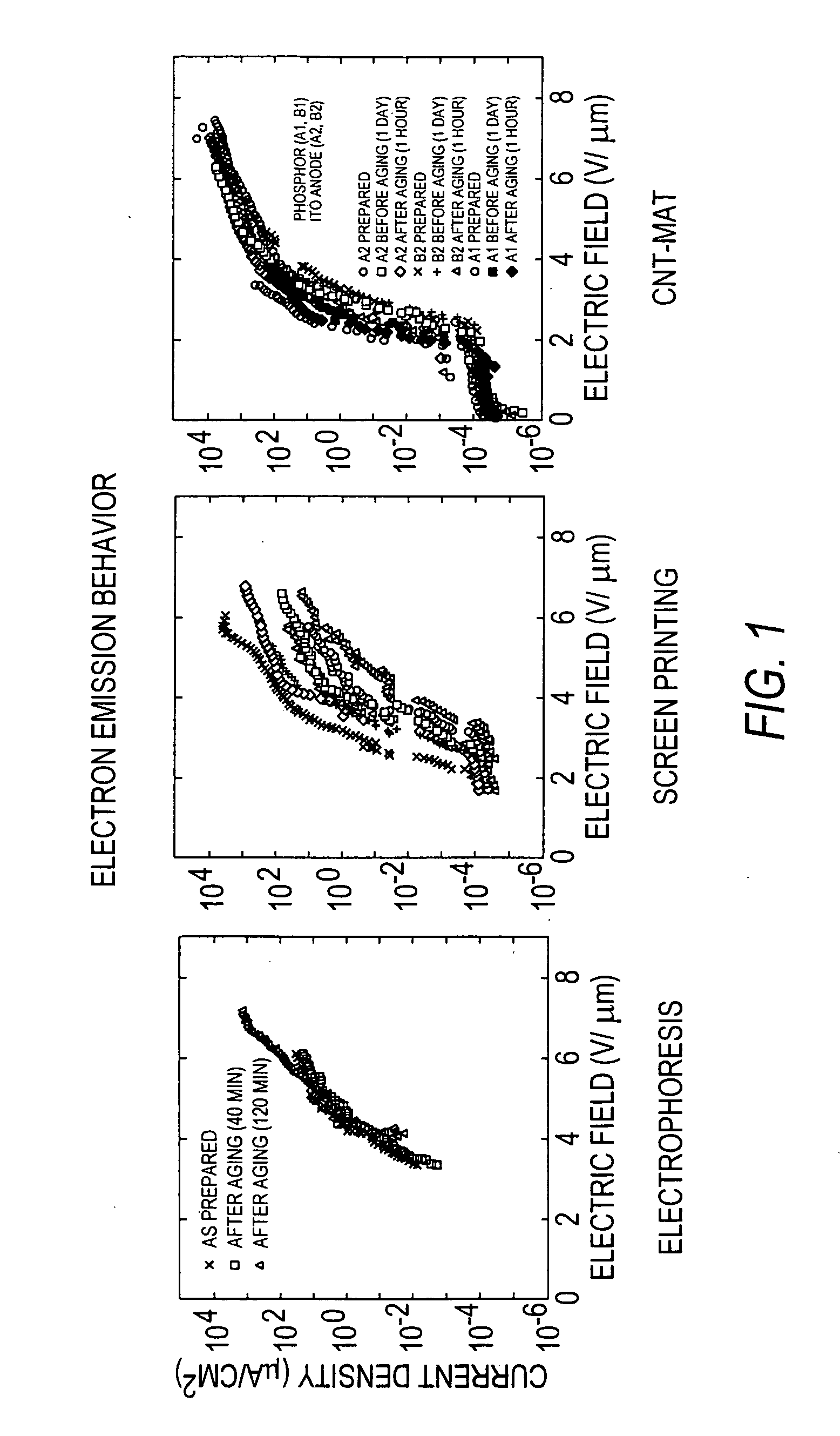
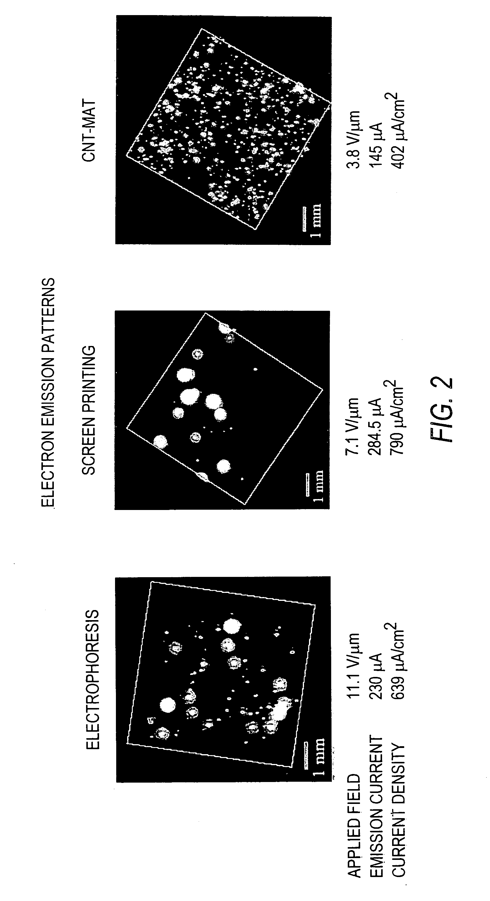
[0089] As shown in FIGS. 3, 4, and 5, the emission characteristics from carbon nanotube (CNT) cathodes made by screen printing on a glass substrate were measured after aging in an ultra high vacuum chamber (5.3×10⁻⁸ Pa). CNT cathodes on the glass substrate were exposed to argon (Ar) plasma with a discharge voltage of 250 V and a vacuum of 40 Pa. The plasma exposure time was varied in following times (30 s, 1 min, 2 min, 3 min, 4 min and 5 min). The emission characteristics from CNT cathodes were measured in an ultra high vacuum chamber. FIG. 3 shows I-V characteristics of CNT cathodes before and after plasma treatment for 3 min. The emission current increased after an Ar plasma treatment for 3 min by three orders of magnitude from 9.0×10⁻⁵ to 0.3 mA / cm2 at 4 V / μm field with a decrease in turn-on voltage from 3.3 V / μm to 1.7 V / μm. FIG. 4 shows electron emission patterns at 4.6 V / μm; (a) before plasma treatment; (b) after plasma treatment for 3 min. This clearly indicates...


PUM


Abstract

Field emission devices comprising carbon nanotube mats which have been treated with laser or plasma are provided. Mats are formed from carbon nanotubes, also known as carbon fibrils, which are vermicular carbon deposits having diameters of less than about one micron. The carbon nanotube mats are then subjected to laser or plasma treatment. The treated carbon nanotube mat results in improved field emission performance as either a field emission cathode or as part of a field emission device.

Description

RELATED APPLICATIONS [0001] This application claims the benefit of U.S. Provisional Application No. 60 / 485,918, filed Jul. 9, 2003. This application is also a continuation in part of PCT / US03 / 19068 filed Jun. 16, 2003, which claims benefit to the U.S. Provisional Application No. 60 / 388,616, filed Jun. 14, 2002. This application is also a continuation in part of U.S. Ser. No. 10 / 171,760, filed Jun. 14, 2002, which claims benefit to the U.S. Provisional Application No. 60 / 298,193, filed Jun. 14, 2001. This application is also a continuation in part of U.S. Ser. No. 10 / 171,773, filed Jun. 14, 2002, which claims benefit to U.S. Provisional Application No. 60 / 298,228, filed Jun. 14, 2001.TECHNICAL FIELD [0002] The present invention relates to field emission devices or field emission cathodes made from or with carbon nanotube mats, films, or inks that have been laser or plasma treated. BACKGROUND Field Emission Devices [0003] Field emission devices are devices that capitalize on the move...

Claims


Application Information

Patent Timeline
IPC IPC(8): H01J1/62H01J63/04
CPCB82Y10/00H01J2201/30469H01J9/025H01J1/304
Inventor TAKAI, MIKIOFISCHER, ALANNGAW, LEINNIU, CHUNMING
Owner HYPERION CATALYSIS INT
Why Eureka
Try Eureka