Electroless cobalt alloy deposition process

a cobalt alloy and deposition process technology, applied in the direction of liquid/solution decomposition chemical coating, metallic material coating process, coating, etc., can solve the problems of not satisfactorily catalyzing or initiating, reducing the reliability of the overall circuit of the formed device, and not being able to follow cu-cmp processes. , to achieve the effect of reducing copper corrosion and improving the initiation delay of capping layer deposition

Inactive Publication Date: 2005-07-28
APPLIED MATERIALS INC
View PDF99 Cites 85 Cited by
  • Summary
  • Abstract
  • Description
  • Claims
  • Application Information

AI Technical Summary

Problems solved by technology

The formation of copper oxides at the interface between metal layers can increase the resistance (e.g., copper interconnects) and reduce the reliability of the overall circuit in the formed device.
Cobalt-containing alloys, such as cobalt tungsten phosphide (CoWP), are materials established to meet many or all requirements and may be deposited by electroless deposition techniques, though copper generally does not satisfactorily catalyze or initiate deposition of these materials from standard electroless solutions.
While deposition of cobalt-containing alloys may be easily initiated electrochemically (e.g., by applying a sufficiently negative potential), a continuous conductive surface over the substrate surface is required and not available following Cu-CMP processes.
However, deposition of the catalytic material may require multiple steps or use of catalytic colloid compounds.
Catalytic colloid compounds may adhere to dielectric materials on the substrate surface and result in undesired, non-selective deposition of the capping alloy material.
Non-selective deposition of metal alloy capping material may lead to surface contamination and eventual device failure from short circuits and other device irregularities.
However, the use of palladium chloride solutions typically results in the formation of clusters of palladium atoms bridged by chlorine atoms.
The selectivity of the subsequent capping layer deposition is deteriorated due to palladium cluster contamination of the dielectric material and ultimate failure of the device.

Method used


Image

  • Electroless cobalt alloy deposition process
  • Electroless cobalt alloy deposition process
  • Electroless cobalt alloy deposition process

Examples


example 1

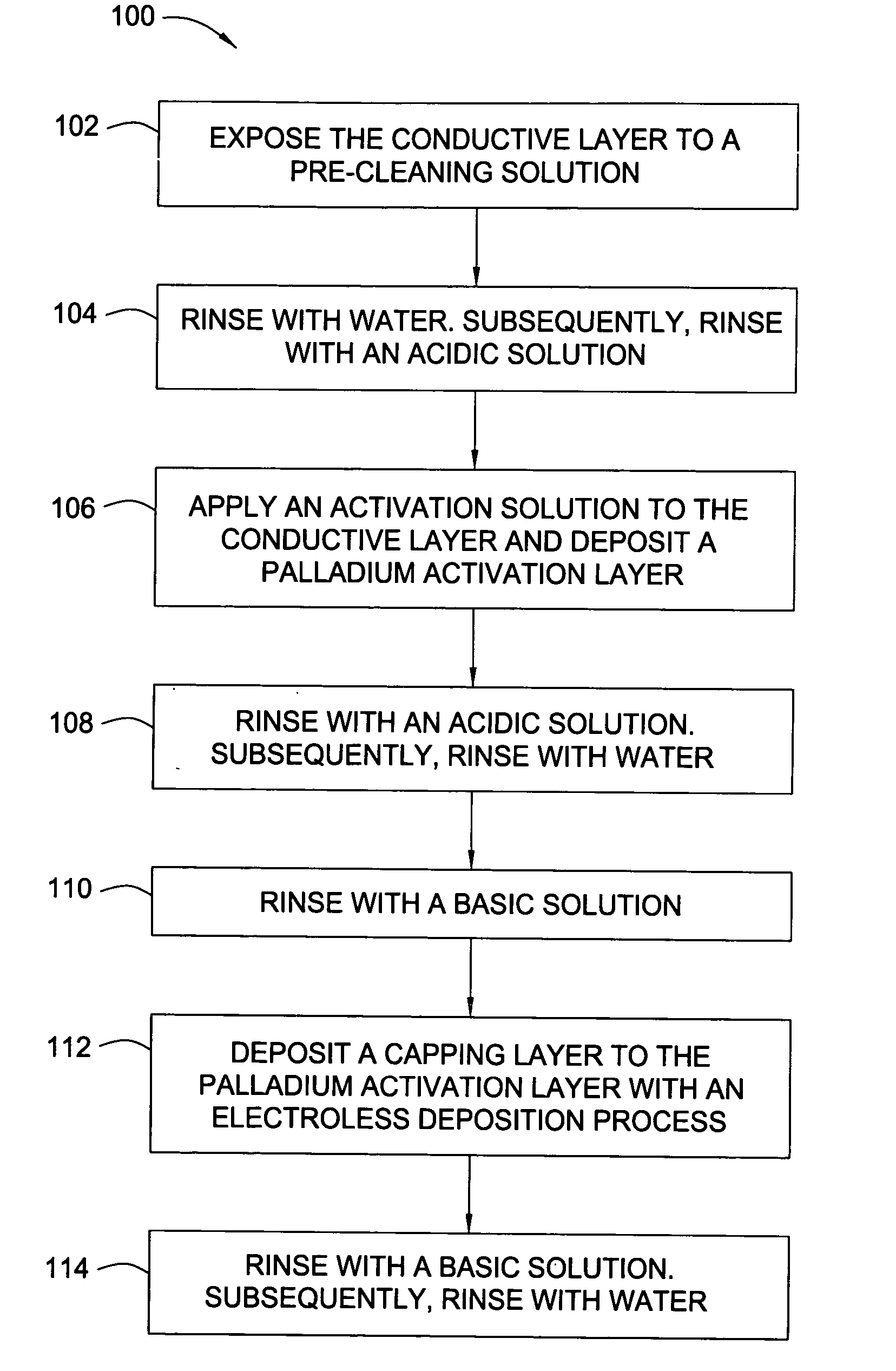
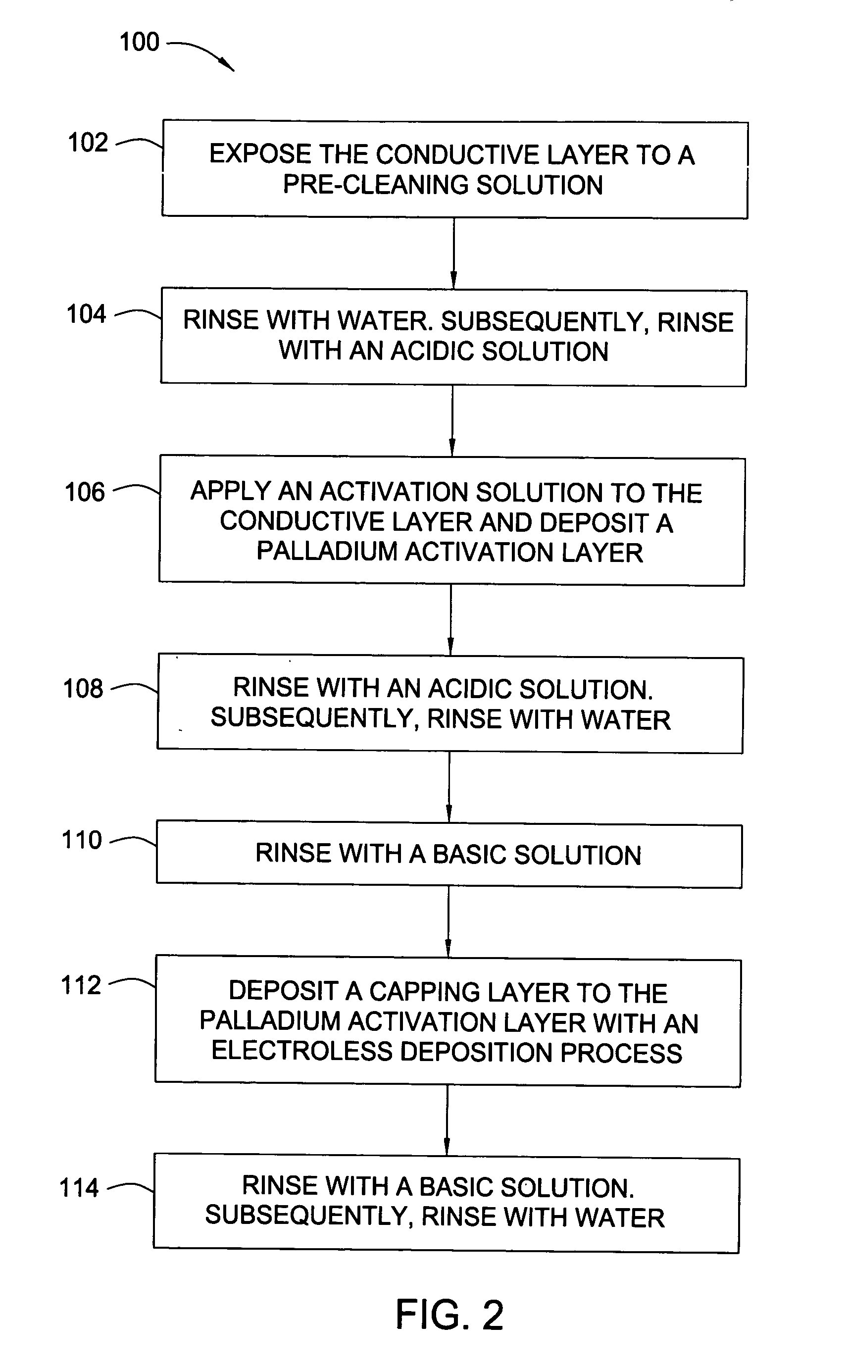
[0064] After a CMP process, a 300 mm substrate containing copper filled features supported by TaN / Ta barrier layers was rinsed with degassed, deionized water, exposed to a complexing solution for 30 seconds and subsequently rinsed with degassed, deionized water for 30 seconds. The substrate was exposed to an acidic wash containing HNO3 with a pH of 2.8. The acidified substrate was exposed for 60 seconds to 200 mL of a palladium activation solution (pH of 2.8) containing 0.04 mM Pd(NO3)2 and 1.0 mM HNO3. The substrate was rinsed with the acid wash and subsequently rinsed with degassed, deionized water for 30 seconds. The rinsed substrate was exposed to a pH basic wash solution containing TMAH for 20 seconds. The basified palladium layer was exposed to an electroless cobalt-containing solution containing 25 mg / L of surfactant (TRITON® 100) and 100 mg / L of ascorbic acid to form a capping layer. The substrate was rinsed with the pH basic wash solution and subsequent degassed, deionized ...

example 2

[0065] After a CMP process, a 300 mm substrate containing copper filled features supported by TaN / Ta barrier layers was rinsed with degassed, deionized water, exposed to a complexing solution for 30 seconds and subsequently rinsed with degassed, deionized water for 30 seconds. The substrate was exposed to an acidic wash containing HNO3 with a pH of 2.5. The acidified substrate was exposed for 40 seconds to 200 mL of a palladium activation solution (pH of 2.5) containing 0.87 mM Pd(NO3)2 and 2.0 mM HNO3. The substrate was rinsed with the acid wash and subsequently rinsed with degassed, deionized water for 30 seconds. The rinsed substrate was exposed to a pH basic wash solution containing TMAH for 20 seconds. The basified palladium layer was exposed to an electroless cobalt-containing solution containing 25 mg / L of surfactant (TRITON® 100) and 100 mg / L of ascorbic acid to form a capping layer. The substrate was rinsed with the pH basic wash solution and subsequent degassed, deionized ...

example 3

[0066] After a CMP process, a 300 mm substrate containing copper filled features supported by TaN / Ta barrier layers was rinsed with degassed, deionized water, exposed to a complexing solution for 30 seconds and subsequently rinsed with degassed, deionized water for 30 seconds. The substrate was exposed to an acidic wash containing HNO3 with a pH of 2.9. The acidified substrate was exposed for 60 seconds to 200 mL of a palladium activation solution (pH of 2.9) containing 0.04 mM Pd(NO3)2 and 1.0 mM methanesulfonic acid. The substrate was rinsed with the acid wash and subsequently rinsed with degassed, deionized water for 30 seconds. The rinsed substrate was exposed to a pH basic wash solution containing TMAH for 20 seconds. The basified palladium layer was exposed to an electroless cobalt-containing solution containing 25 mg / L of surfactant (TRITON® 100) and 100 mg / L of ascorbic acid to form a capping layer. The substrate was rinsed with the pH basic wash solution and subsequent dega...


PUM

PropertyMeasurementUnit
concentrationaaaaaaaaaa
exposure timeaaaaaaaaaa

Abstract

In one embodiment, a method for depositing a cobalt-containing capping layer on a metal layer is provided which includes rinsing the metal layer with a deionized water wetting step, depositing a palladium layer on the metal layer by exposing the metal layer to an electroless activation solution comprising a palladium precursor and an acid, and depositing the cobalt-containing capping layer on the palladium layer by exposing the palladium layer to an electroless cobalt-containing solution comprising a cobalt source, a tungsten source, an oxygen scavenger and a surfactant. Ascorbic acid may be used as the oxygen scavenger. In another embodiment, a composition of an electroless plating solution is provided which includes a cobalt source at a concentration in a range from about 50 mM to about 250 mM, a tungsten source at a concentration in a range from about 10 mM to about 100 mM, a complexing agent at a concentration in a range from about 10 mM to about 200 mM, at least one reductant at a concentration in a range from about 1 mM to about 100 mM, a surfactant at a concentration in a range from about 1 mg / L to about 100 mg / L, and ascorbic acid at a concentration in a range from about 30 mg / L to about 300 mg / L.

Description

CROSS-REFERENCE TO RELATED APPLICATIONS [0001] This application claims benefit of U.S. Provisional Patent Application Ser. No. 60 / 539,544, filed Jan. 26, 2004, which is herein incorporated by reference.BACKGROUND OF THE INVENTION [0002] 1. Field of the Invention [0003] Embodiments of the invention generally relate to methods for depositing capping layers on a feature formed as part of an electronic device, and more particularly to methods for activating a conductive surface on the feature and subsequently depositing the capping layer on the activated conductive surface. [0004] 2. Description of the Related Art [0005] Recent improvements in circuitry of ultra-large scale integration (ULSI) on substrates indicate that future generations of semiconductor devices will require multi-level metallization with smaller geometric dimensions. The multilevel interconnects that lie at the heart of this technology require planarization of interconnect features formed in high aspect ratio features...

Claims


Application Information

Patent Timeline
Patent Type & Authority Applications(United States)
IPC IPC(8): C23C18/18C23C18/34C23C18/50C25D5/10H01L21/288H01L21/768
CPCC23C18/34C23C18/50C23C18/1844H01L21/76849H01L21/76874H01L21/288
Inventor FANG, HONGBINEMAMI, RAMINWEIDMAN, TIMOTHYSHANMUGASUNDRAM, ARULKUMAR
Owner APPLIED MATERIALS INC
Why Eureka
Try Eureka