Electromagnetic radiation sensor and method for fabricating the same

a technology of electromagnetic radiation and electromagnetic sensor, which is applied in the direction of photometry using electric radiation detectors, optical radiation measurement, instruments, etc., can solve the problems of large amount of incident electromagnetic radiation reflected by metal film, increase the fabrication cost, and significantly reduce the mechanical strength of film, etc., to achieve easy fabrication and high sensitivity

Inactive Publication Date: 2005-07-28
FUJITSU LTD
View PDF14 Cites 10 Cited by
  • Summary
  • Abstract
  • Description
  • Claims
  • Application Information

AI Technical Summary

Benefits of technology

[0015] It is an object of the present invention to provide an electromagnetic sensor which is easy to fabricate and has high sensitivity while the mechanical strength is ensured, an electromagnetic radiation detecting device including the same, and a method for fabricating the same.

Problems solved by technology

However, a thin-film electromagnetic radiation sensor having the MSM structure or MIM structure using these metals has the drawback that a large amount of incident electromagnetic radiation is reflected by a metal film.
Unfortunately, the formation of the antireflection film increases the fabrication cost.
Also, as described in U.S. Pat. No. 6,399,946, in the method in which the thickness of the metal film which functions as a top electrode is decreased to a few nanometers, if the thickness of the metal film which functions not only as an absorbent but also as a top electrode decreases to a few nanometers, the mechanical strength of the film significantly lowers, and other problem arises.
In addition, it is extremely difficult to evenly form a thin film having a thickness of a few nanometers within the range of area of square centimeter order.
Furthermore, as described in U.S. Pat. No. 6,399,946, the fabrication method of giving the metal film a two-layered structure is complicated, so the cost rises, or the yield lowers.
However, even this infrared detecting element cannot have sufficient sensitivity if a metal, such as Au, having high conductivity is used as the top electrode.
Also, the fabrication is complicated because a layer which serves as the infrared absorbing portion must be formed on the top electrode.

Method used


Image

  • Electromagnetic radiation sensor and method for fabricating the same
  • Electromagnetic radiation sensor and method for fabricating the same
  • Electromagnetic radiation sensor and method for fabricating the same

Examples


first embodiment

[0035] The first embodiment of the present invention will be described below. FIG. 3 is a schematic view showing the structure of a thin-film electromagnetic radiation sensor according to the first embodiment of the present invention.

[0036] In a thin-film electromagnetic radiation sensor 1, an SiO2 layer 3, Ti layer 4, Pt layer 5, PLZT ((Pb,La)(Zr,Ti)O3) layer 6, and IrO2 layer 7 are sequentially formed on an Si substrate 2. The thicknesses of the Ti layer 4, Pt layer 5, PLZT ((Pb,La)(Zr,Ti)O3) layer 6, and IrO2 layer 7 are, for example, about 20 nm, 100 nm, 200 nm, and 100 nm, respectively.

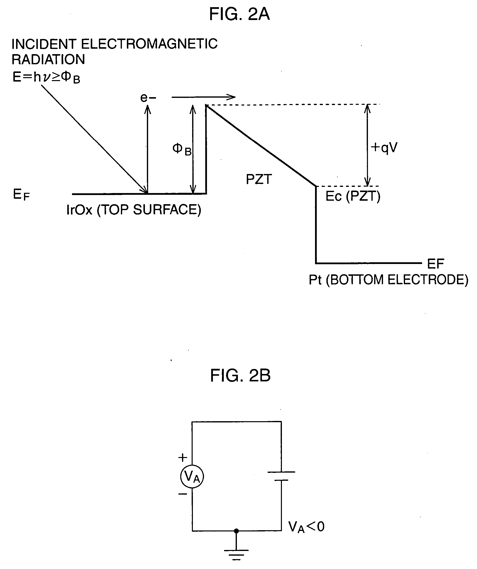
[0037] Although the Ti layer 4 is formed as an adhesive layer which adheres the Pt layer 5 as a bottom electrode and the Si substrate 2, the Ti layer 4 also functions as a part of the bottom electrode. The PLZT layer 6 is a ferroelectric layer and formed by, for example, a sol-gel method, RF sputtering method, or metal organic CVD (MOCVD) method. The IrO2 layer 7 functions as a top electrode. T...

second embodiment

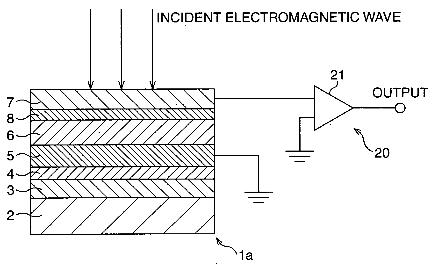
[0042] The second embodiment of the present invention will be described below. FIG. 4 is a schematic view showing the structure of a thin-film electromagnetic radiation sensor according to the second embodiment of the present invention.

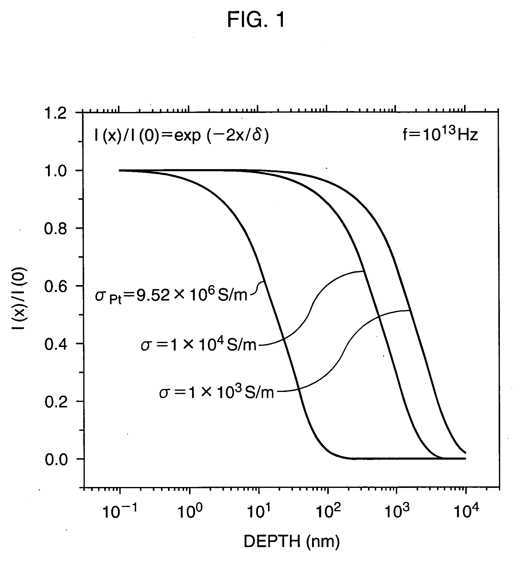
[0043] A thin-film electromagnetic radiation sensor 1a differs from the thin-film electromagnetic radiation sensor 1 according to the first embodiment in that a Pt layer 8 is formed between a PLZT layer 6 and IrO2 layer 7. The thickness of the Pt layer 8 is equal to or smaller than a skin depth, and is about 5 nm, for example. The Pt layer 8 is formed by DC sputtering method.

[0044] In the thin-film electromagnetic radiation sensor 1a having the above arrangement, the presence of the Pt layer 8 makes the height of a barrier higher by about 0.8 eV to 1 eV than that in the thin-film electromagnetic radiation sensor 1.

[0045] Note that in the fabrication of the thin-film electromagnetic radiation sensor 1a, it is preferable to form the Pt layer 8 and Ir...

third embodiment

[0047] The third embodiment of the present invention will be described below. FIG. 5 is a schematic view showing the structure of a thin-film electromagnetic radiation sensor according to the third embodiment of the present invention.

[0048] In a thin-film electromagnetic radiation sensor 1b, an SrTiO3 layer 16 and IrO2 layer 7 are sequentially formed on an n-type Si substrate 12. The thickness of the SrTiO2 layer 16 is, for example, about 100 nm. The SrTiO3 layer 16 is formed by pulse laser deposition method or RF magnetron sputtering method, for example.

[0049] In this embodiment, the n-type Si substrate 12 functions as a bottom electrode, and the IrO2 layer 7 functions as a top electrode.

[0050] The same effects as the first embodiment can also be obtained by the thin-film electromagnetic radiation sensor 1b having the above arrangement.


PUM


Abstract

An SiO2 layer (3), a Ti layer (4), a Pt layer (5), a PLZT layer (6) and an IrO2 layer (7) are formed sequentially on an Si substrate (2). The IrO2 layer (7) functioning as a top electrode has a thickness of about 100 nm. Since the IrO2 layer (7) has conductivity lower than that of Pt or the like conventionally used as a top electrode and a skin depth deeper than that of Pt or the like, sufficient sensitivity can be attained by a thickness of about 100 nm.

Description

CROSS-REFERENCE TO RELATED APPLICATIONS [0001] This application is based upon and claims the benefit of priority from the prior PCT International Patent Application No. PCT / JP03 / 02704, filed on Mar. 7, 2003, the entire contents of which are incorporated herein by reference.TECHNICAL FIELD [0002] The present invention relates to an electromagnetic radiation sensor, such as a photosensor or infrared sensor, which detects incident electromagnetic radiation and converts this electromagnetic radiation into an electrical signal, and a method for fabricating the same. BACKGROUND ART [0003] An electromagnetic radiation sensor having, for example, an MSM (Metal-Semiconductor-Metal) structure, MIM (Metal-Insulator-Metal) structure, or MIS (Metal-Insulator-Semiconductor) structure formed by stacking thin films is widely used as a photosensor of a reader of a CD-ROM, DVD-ROM, or the like, a heat sensor using infrared radiation, or a motion detector. When electromagnetic radiation is incident on...

Claims


Application Information

Patent Timeline
Patent Type & Authority Applications(United States)
IPC IPC(8): G01J1/42G01J5/02H01L31/101H01L37/02
CPCG01J1/42H01L37/02H01L31/101H10N15/10
Inventor BANIECKI, JOHN DAVIDSHIOGA, TAKESHIKURIHARA, KAZUAKI
Owner FUJITSU LTD
Why Eureka
Try Eureka