Transistor with doped gate dielectric

a technology of doped gate dielectric and transistor, which is applied in the direction of semiconductor devices, basic electric elements, electrical apparatus, etc., can solve the problems of reducing the speed and performance of transistors with high k gate dielectric materials, affecting affecting the use of thin oxides in many device applications. , to achieve the effect of improving the electrical performance of transistors, improving voltage stability, and increasing speed

Active Publication Date: 2005-08-04
INFINEON TECH AG
View PDF12 Cites 19 Cited by
  • Summary
  • Abstract
  • Description
  • Claims
  • Application Information

AI Technical Summary

Benefits of technology

[0011] Advantages of the preferred embodiments of the present invention include providing a transistor design and manufacturing method thereof wherein the electrical performance of the transistor is improved. The transistor has increased speed, improved voltage stability, and increased electron and hole mobility. The dopant species fill vacancies in the gate dielectric, removing defects in the gate dielectric material, eliminating leakage paths and improving the transistor's performance. The gate dielectric is doped using processes that are compatible with semiconductor device manufacturing process flows, and that are easily implemented into existing manufacturing process flows.

Problems solved by technology

However, as devices are scaled down in size, silicon dioxide becomes a problem because of gate leakage current, which can degrade device performance.
For low power logic (for portable electronic applications, for example), the main issue is low leakage current, which is necessary in order to extend battery life.
However, the resulting gate leakage currents make the use of such thin oxides impractical in many device applications where low standby power consumption is required.
However, the device performance of using high k dielectric materials suffers from trapped charge in the dielectric layer which deteriorates the mobility, making the drive current lower than in transistors having silicon dioxide gate oxides, and hence reducing the speed and performance of transistors having high k gate dielectric materials.
While this method provides increased hole mobility, it requires plasma processes which can be difficult to work with and may cause damage to the devices manufactured, as well as requiring an additional tool for the plasma processing.

Method used


Image

  • Transistor with doped gate dielectric
  • Transistor with doped gate dielectric
  • Transistor with doped gate dielectric

Examples


Embodiment Construction

[0020] The making and using of the presently preferred embodiments are discussed in detail below. It should be appreciated, however, that the present invention provides many applicable inventive concepts that can be embodied in a wide variety of specific contexts. The specific embodiments discussed are merely illustrative of specific ways to make and use the invention, and do not limit the scope of the invention.

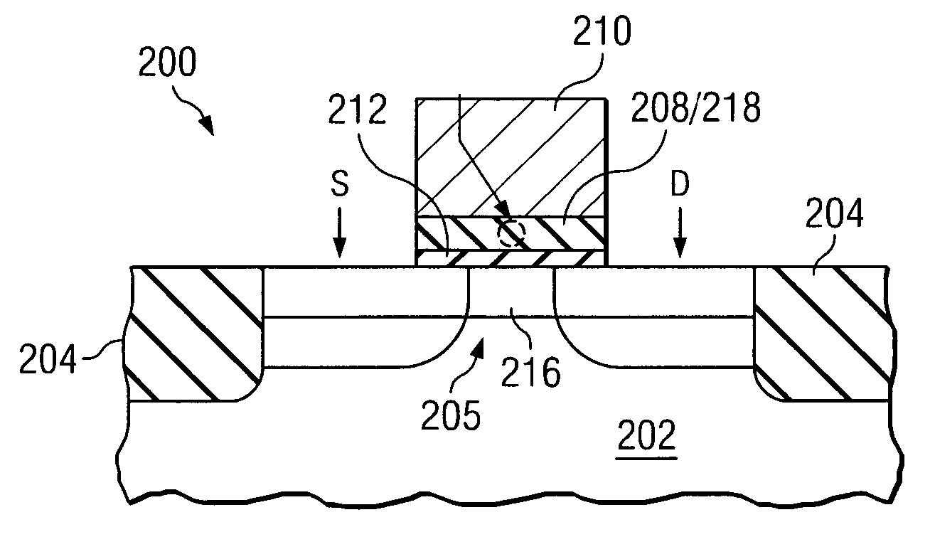
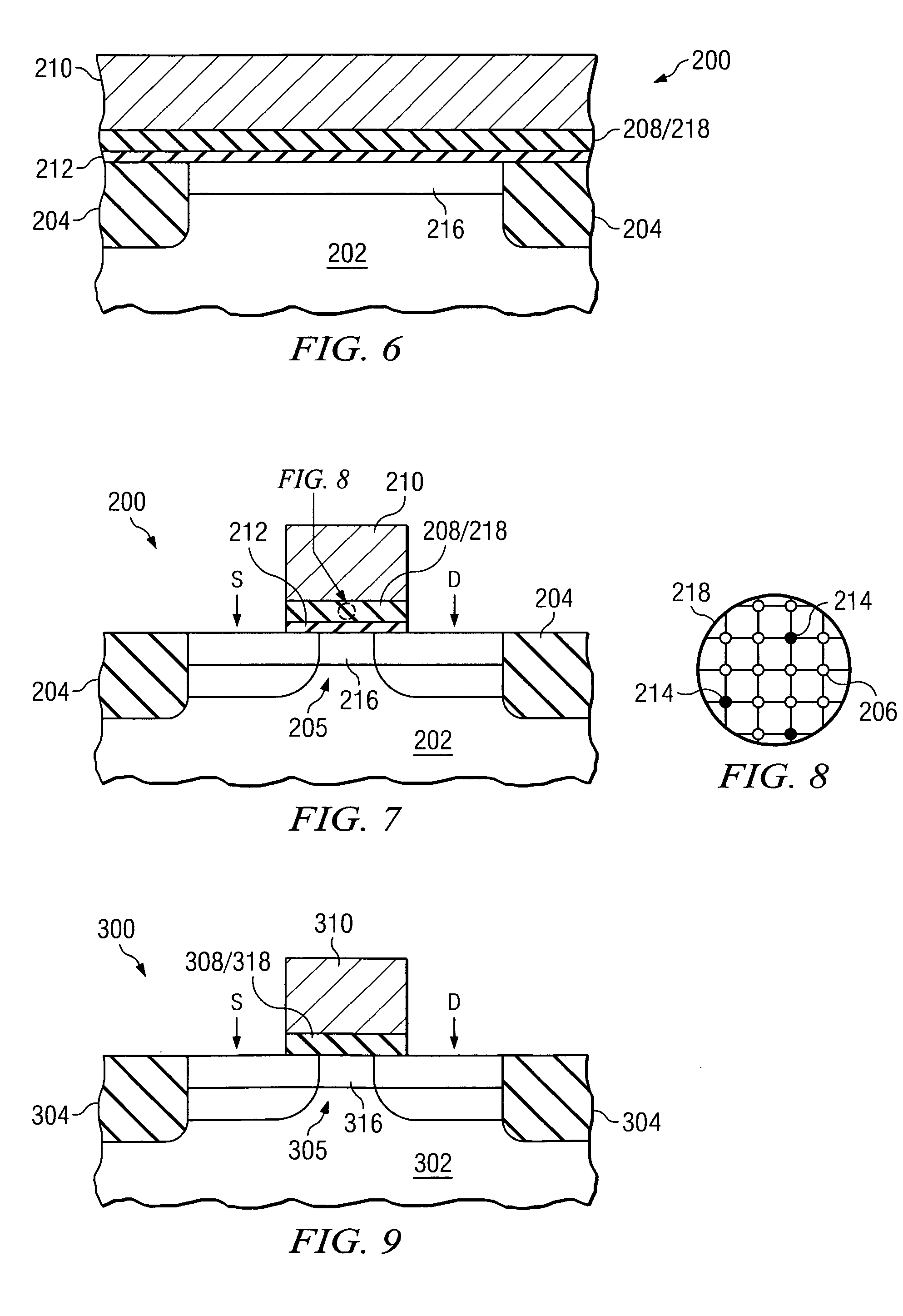
[0021] The present invention will be described with respect to preferred embodiments in a specific context, namely a transistor formed on a semiconductor device. The invention may also be applied, however, to MOSFETs or other transistor devices, and may include PMOS, NMOS, or CMOS devices, as examples. Only one transistor is shown in each of the figures; however, there may be many transistors formed on the semiconductor devices shown.

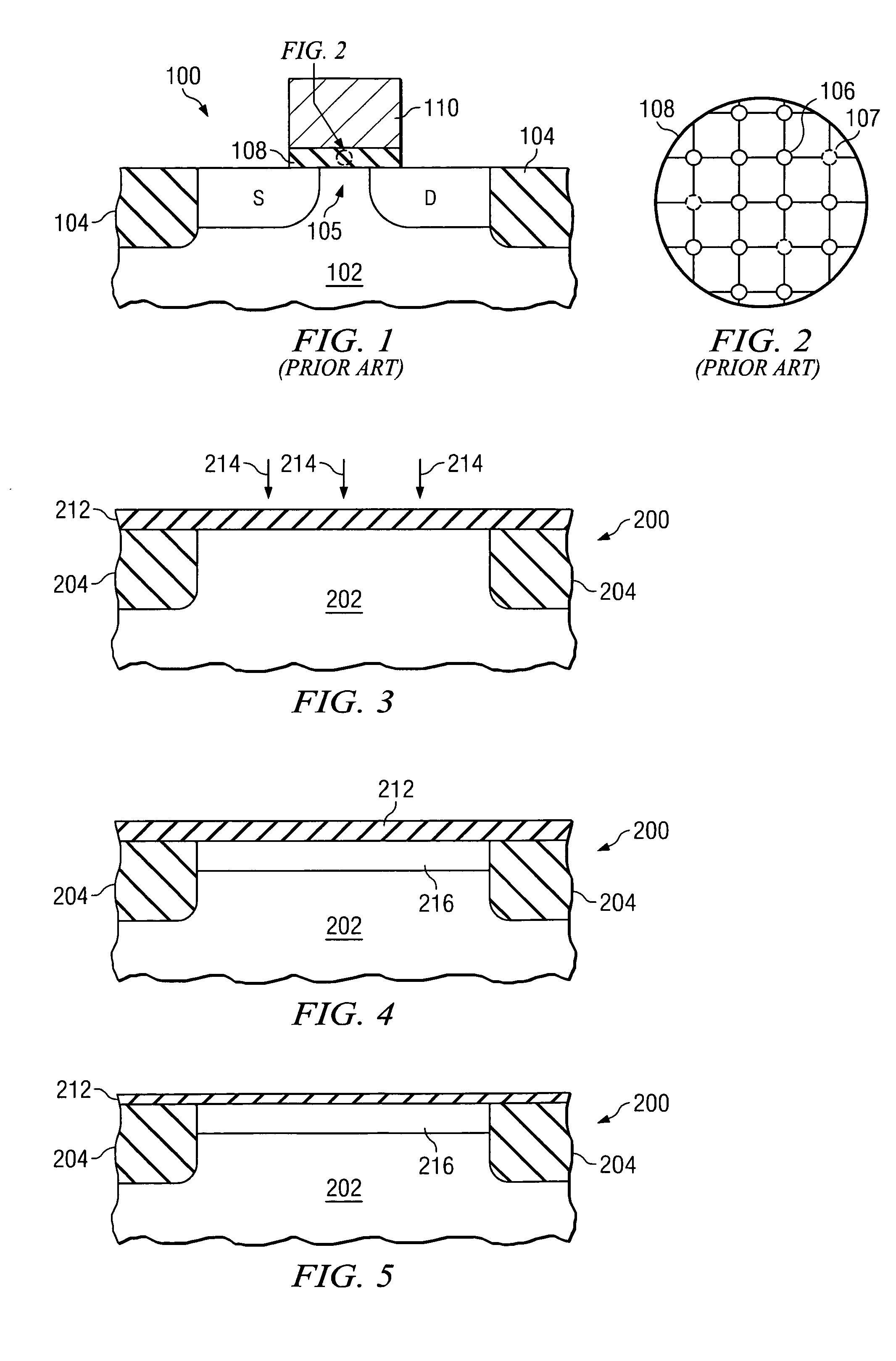
[0022]FIG. 1 shows a cross-sectional view of a prior art transistor 100 formed over a workpiece 102. After shallow trench isolation (STI) reg...


PUM


Abstract

A transistor and method of manufacture thereof. A semiconductor workpiece is doped before depositing a gate dielectric material. Using a separate anneal process or during subsequent anneal processes used to manufacture the transistor, dopant species from the doped region of the workpiece are outdiffused into the gate dielectric, creating a doped gate dielectric. The dopant species fill vacancies in the atomic structure of the gate dielectric, resulting in a transistor having increased speed, reduced power consumption, and improved voltage stability.

Description

TECHNICAL FIELD [0001] The present invention relates generally to semiconductor devices, and more particularly to a method of fabricating a transistor and a structure thereof. BACKGROUND [0002] Semiconductor devices are used in a variety of electronic applications, such as personal computers, cell phones, digital cameras, and other electronic equipment, as examples. A transistor is an element that is utilized extensively in semiconductor devices. There may be millions of transistors on a single integrated circuit (IC), for example. A common type of transistor used in semiconductor device fabrication is a metal oxide semiconductor field effect transistor (MOSFET). [0003] The gate dielectric for MOSFET devices has in the past typically comprised silicon dioxide. However, as devices are scaled down in size, silicon dioxide becomes a problem because of gate leakage current, which can degrade device performance. Therefore, there is a trend in the industry towards the development of the u...

Claims


Application Information

Patent Timeline
Patent Type & Authority Applications(United States)
IPC IPC(8): H01L21/265H01L21/28H01L21/324H01L21/336H01L29/51
CPCH01L21/26506H01L21/28176H01L21/28185H01L29/66545H01L21/324H01L29/517H01L29/518H01L21/28194H01L21/26513
Inventor LI, HONG-JYH
Owner INFINEON TECH AG
Why Eureka
Try Eureka