Amplifier arrangement and method for calibrating an amplifier arrangement

Inactive Publication Date: 2005-08-04
INTEL CORP
6 Cites 8 Cited by

AI-Extracted Technical Summary

Problems solved by technology

The fact that such transceivers do not perform any intermediate-frequency processing means that it is necessary to distribute the gain control over the baseband signal processing and the radio-frequency signal processing.
In addition, the gain control cannot respectively be effected before the actual transmission timeslots, as in the case of time-division multiple access systems, but rather needs to be performed during the continuous user-data transmission.
In addition, it is a complex matter to ensure exactly 20 dB of gain in the receiver's LNA regardless of t...

Method used

[0056] The gain control loops described in FIG. 1 allow self-calibration of the PGC in baseband and radio-frequency parts. This allows highly accurate coverage of a wide dynamic range of far beyond 60 dB. In addition, good carrier frequenc...

Benefits of technology

[0035] The fact that the programmable gain control uses a digital data format, in one example, means that it is very robust toward radiated interference.
[0036] In comparison to automatic gain control, the programmable gain control allows a higher level of flexibility for the choice of amplifier stages and for adjusting the time between the baseband gain control and the radio-frequency gain control. In addition, a large number of different baseband ICs can be combined with radio-frequency ICs from different manufacturers, which advantageously increases flexibility.
[0037] In CDMA systems, the reference variable for the gain control during transmitter power control in the baseband chip is generated on the basis of the measured reception power and the control bits which are received from the base station. In this case, the transmission power levels sent are specified in 1-dB steps with an accu...

Abstract

An amplifier arrangement is disclosed that includes at least two series-connected, programmable amplifiers. The amplifiers each have a different amplifier step size. In addition, a calibration path is provided which feeds back the output of the second programmable amplifier to the programming inputs of the first and/or second programmable amplifier. The calibration path includes an analog/digital converter and an evaluation and control element. It is thus possible to calibrate away less-than-ideal characteristics, particularly in the case of changes in the gain from one amplifier block to another. The proposed amplifier arrangement and the method for calibration are particularly suitable for use in transmission and reception paths in transceivers which operate continuously over time.

Application Domain

Negative-feedback-circuit arrangementsElectric devices +6

Technology Topic

TransceiverEngineering +4

Image

  • Amplifier arrangement and method for calibrating an amplifier arrangement
  • Amplifier arrangement and method for calibrating an amplifier arrangement
  • Amplifier arrangement and method for calibrating an amplifier arrangement

Examples

  • Experimental program(1)

Example

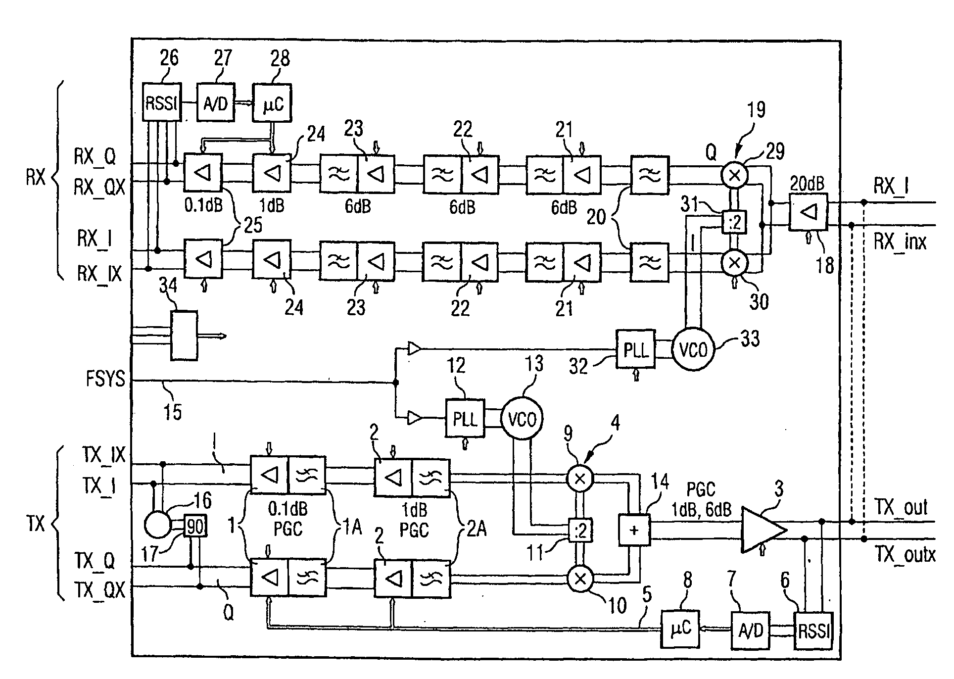
[0048]FIG. 1 shows an amplifier arrangement 1, 2, 3, 5 in accordance with the present invention both in the transmission path Tx and in the reception path Rx of a mobile radio transceiver. In the transmission path Tx, the amplifier arrangement 1, 2, 3, 5 comprises a programmable amplifier 1, a programmable amplifier 2 and a programmable amplifier 3. The programmable amplifier 1 is provided both in the inphase path I and in the quadrature path Q of the baseband signal processing chain. On the output side, the programmable amplifier 1 comprises a respective low-pass filter 1A. The programmable amplifier 1 has a further programmable amplifier 2 arranged downstream of it, likewise respectively split into the inphase and quadrature paths I, Q.
[0049] The programmable amplifier 2 likewise comprises a respective low-pass filter 2A on the output side. The outputs of the programmable amplifiers 2 have an upward frequency converter 4 connected to them which results in frequency conversion from baseband to a radio frequency. At the output of the frequency converter 4 there is a programmable amplifier 3 whose output forms the output of the amplifier arrangement 1, 2, 3, 5.
[0050] The amplifier arrangement 1, 2, 3, 5 also comprises a calibration path 5 which couples the output of the programmable amplifier 3 to programming inputs of the programmable amplifiers 1 and of the programmable amplifiers 2. The calibration path comprises, as a level detector, a means for outputting a reception-field strength indicator signal 6 whose input is connected to the output of the programmable amplifier 3. The output of the means for outputting a reception field indicator signal 6 is coupled to a microcontroller 8 via an analog/digital converter 7. In turn, the output of the microcontroller 8 is connected to the programming inputs of the programmable amplifiers 1, 2.
[0051] The frequency converter 4 comprises two frequency mixers 9, 10 whose first inputs are respectively connected to outputs of the programmable amplifiers 2. Second inputs of the frequency mixers 9, 10 are coupled to the output of a phase locked loop 12 with an oscillator 13 via a frequency and phase divider 11. The outputs of the frequency mixers 9, 10 are connected to the input of the programmable amplifier 3 via an adding element 14. The input of the phase locked loop 12 is connected to a reference frequency input 15 of the transceiver circuit Rx, Tx. The entire signal processing chain in the transmission path Tx is respectively designed using symmetrical circuitry in the baseband path and in the radio-frequency path and is designed to carry difference signals. In addition, a test signal generator 16 is coupled to the inputs of the first programmable amplifiers 1. The test signal generator 16 is connected to the programmable amplifier 1 in the inphase path I directly, whereas it is connected to the programmable amplifier 1 in the quadrature path Q via a 90° phase shifter 17.
[0052] The programmable amplifiers 1 can be programmed in steps of 0.1 dB. The programmable amplifiers 2 can be programmed in steps of 1 dB. The programmable amplifier 3 can be programmed in steps of either 1 dB or 6 dB.
[0053] In addition to the described amplifier arrangement 1, 2, 3, 5 based on the proposed principle in the transmission path Tx, a further amplifier arrangement 18, 21, 22, 23, 24, 25, 26, 27, 28 in accordance with the present invention is provided in the reception path Rx. A programmable amplifier 18 is designed as a low-noise preamplifier (LNA, Low-Noise Amplifier) and forms the input of the reception signal change shown. The output of the programmable amplifier 18 is connected to a downward frequency converter 19. The downward frequency converter 19 has an inphase output and a quadrature output. Connected to these outputs via a respective low-pass filter 20 in the inphase and quadrature paths I, Q is a respective amplifier chain comprising a programmable amplifier 21, a programmable amplifier 22, a programmable amplifier 23, a programmable amplifier 24 and a programmable amplifier 25.
[0054] There is also a calibration path 26, 27, 28 which couples the outputs of the programmable amplifiers 25 to respective programming inputs of the programmable amplifiers 24, 25. In a similar manner to the calibration path 5, the calibration path comprises a level detector 26, which is designed as a reception-field strength indicator, with a downstream analog/digital converter 27 and a microcontroller 28. The output side of the programmable amplifiers 21, 22, 23 has a respective low-pass filter. Whereas the programmable amplifier 18 can be programmed in a stage of 20 dB, the programmable amplifiers 21 to 23 can be programmed in steps of 6 dB. The programmable amplifiers 24 have a step size of 1 dB. The programmable amplifiers 25 have a step size of 0.1 dB.
[0055] The downward frequency converter 19 is designed for frequency conversion of a radio frequency to baseband and, to this end, comprises two frequency mixers 29, 30 whose first inputs are connected to the output of the programmable amplifier 18. Further inputs of the frequency mixers 29, 30 are coupled to a phase locked loop 32 with a voltage-controlled oscillator 33 via a frequency and phase divider 31. The phase locked loop 32 is connected to the reference frequency input 15 for the purpose of supplying a reference frequency. To provide a reference variable for the gain control with the programmable amplifiers, a three-wire bus interface 34 is provided in the transceiver shown in FIG. 1, said three-wire bus interface being coupled to the gain control loops 1, 2, 3, 5; 18, 21, 22, 23, 24, 25, 26, 27, 28 in the transmission and reception paths Tx, Rx.
[0056] The gain control loops described in FIG. 1 allow self-calibration of the PGC in baseband and radio-frequency parts. This allows highly accurate coverage of a wide dynamic range of far beyond 60 dB. In addition, good carrier frequency suppression can also be provided in the radio-frequency part on account of the gain control. Any inaccuracies in the tuning between the individual gain control blocks can easily be substantially reduced or eliminated through calibration.
[0057] In summary, the invention is directed to self-calibration of inaccuracies in programmable amplifiers in the radio-frequency part through fine tuning in baseband using a gain control loop with PGC (Programmable Gain Control). The inaccuracy in the gain may be caused, by way of example, by the relatively large gain step of 20 dB in the low noise amplifier 18 in the receiver Rx or by the IQ modulator 4 in the transmitter.
[0058] In addition, the present invention provides for self-calibration of a combination of two different amplifier stages, for example an amplifier with a step size of 6 dB in combination with an amplifier with a step size of 1 dB. These two amplifiers may either both be provided in the radio-frequency part, may both be provided in baseband or may be provided in a form distributed over the radio-frequency part and baseband, and both in the receiver and in the transmitter.
[0059]FIG. 2 uses exemplary illustrations to show the calibration of programmable amplifiers according to the present invention, in the top half of the figure using an example of a radio-frequency path and in the bottom half of the figure using an example of a baseband signal path. The top left shows the ideal step size for a programmable amplifier in the radio-frequency part of a radio transmitter with programmable gain. To the right of that, the actual step size of a programmable amplifier in the radio-frequency part is indicated by way of example. The less-than-ideal characteristics of the step size, which are shown to an excessive degree, may arise, by way of example, when different programmable amplifiers or amplifiers with different step sizes clash at changeover points, for example at the changeover point from the step size 5×1 dB to the step size 1×6 dB. If this real PGC step size is corrected in baseband through appropriate calibration, as in the present invention, then a practically ideal curve is obtained with amplifier step sizes of equal magnitude, as shown at the far right.
[0060] A further example is shown in the bottom half of FIG. 2. There, an amplifier with a step size of 1 dB in baseband is combined with an amplifier with a step size of 6 dB, likewise in baseband. At the changeover point from one amplifier to the other, combination errors arise which can easily be calibrated away using the present invention.
[0061]FIG. 3 is a diagram that illustrates the relative errors plotted over the change in the step size of the programmable gain, using the example of 0 to 45 dB with a respective step size of 1 dB. It is possible to see that following performance of the calibration the relative error has a very smooth, homogeneous profile for combined PGC step sizes of 1-dB and 6-dB steps.
[0062] By contrast, FIG. 4 is a curve that illustrates the relative errors over the PGC step size in steps of 1 dB, likewise from 1 to 45 dB, without calibration. In this case too, the programmable gain is made up of steps of step size 1 dB and 6 dB, which are generated using different amplifier stages. It is possible to see that large relative errors may arise particularly when transferring from 5 dB in single steps of 1 dB to a step size of 6 dB and back to 6+1 dB without calibration.
[0063] While the invention has been illustrated and described with respect to one or more implementations, alterations and/or modifications may be made to the illustrated examples without departing from the spirit and scope of the appended claims. In particular regard to the various functions performed by the above described components or structures (assemblies, devices, circuits, systems, etc.), the terms (including a reference to a “means”) used to describe such components are intended to correspond, unless otherwise indicated, to any component or structure which performs the specified function of the described component (e.g., that is functionally equivalent), even though not structurally equivalent to the disclosed structure which performs the function in the herein illustrated exemplary implementations of the invention. In addition, while a particular feature of the invention may have been disclosed with respect to only one of several implementations, such feature may be combined with one or more other features of the other implementations as may be desired and advantageous for any given or particular application. Furthermore, to the extent that the terms “including”, “includes”, “having”, “has”, “with”, or variants thereof are used in either the detailed description and the claims, such terms are intended to be inclusive in a manner similar to the term “comprising”.

PUM

no PUM

Description & Claims & Application Information

We can also present the details of the Description, Claims and Application information to help users get a comprehensive understanding of the technical details of the patent, such as background art, summary of invention, brief description of drawings, description of embodiments, and other original content. On the other hand, users can also determine the specific scope of protection of the technology through the list of claims; as well as understand the changes in the life cycle of the technology with the presentation of the patent timeline. Login to view more.

Similar technology patents

Method and device for controlling control operation

InactiveCN103927080Aincrease flexibilitySolve the thumb blind spot
Owner:XIAOMI INC

Self-cleaning control method of cleaning equipment, cleaning equipment and storage medium

InactiveCN111358342Aincrease flexibilityImprove self-cleaning effect
Owner:TIANKE INTELLIGENT TECH CO LTD

Data filter and combination method

InactiveCN101902335Aincrease flexibilitysimple interface
Owner:BEIJING VENUS INFORMATION TECH +1

Classification and recommendation of technical efficacy words

  • high level
  • increase flexibility

Front illuminated back side contact thin wafer detectors

InactiveUS7057254B2reduce radiation damage susceptibilityincrease flexibility
Owner:OSI OPTOELECTRONICS

Security guarantee method and system for Windows terminals based on auto white list

InactiveCN101650768Aincrease flexibilityImprove the range of adaptation
Owner:SHENZHEN Y& D ELECTRONICS CO LTD

Data processing method and system

InactiveUS20070018986A1increase flexibility
Owner:IBM CORP
Why Eureka
Try Eureka