Flowthrough device for multiple discrete binding reactions
- Summary
- Abstract
- Description
- Claims
- Application Information
AI Technical Summary
Benefits of technology
Problems solved by technology
Method used
Image
Examples
example 1
Nanochannel Glass (NCG) Wafers
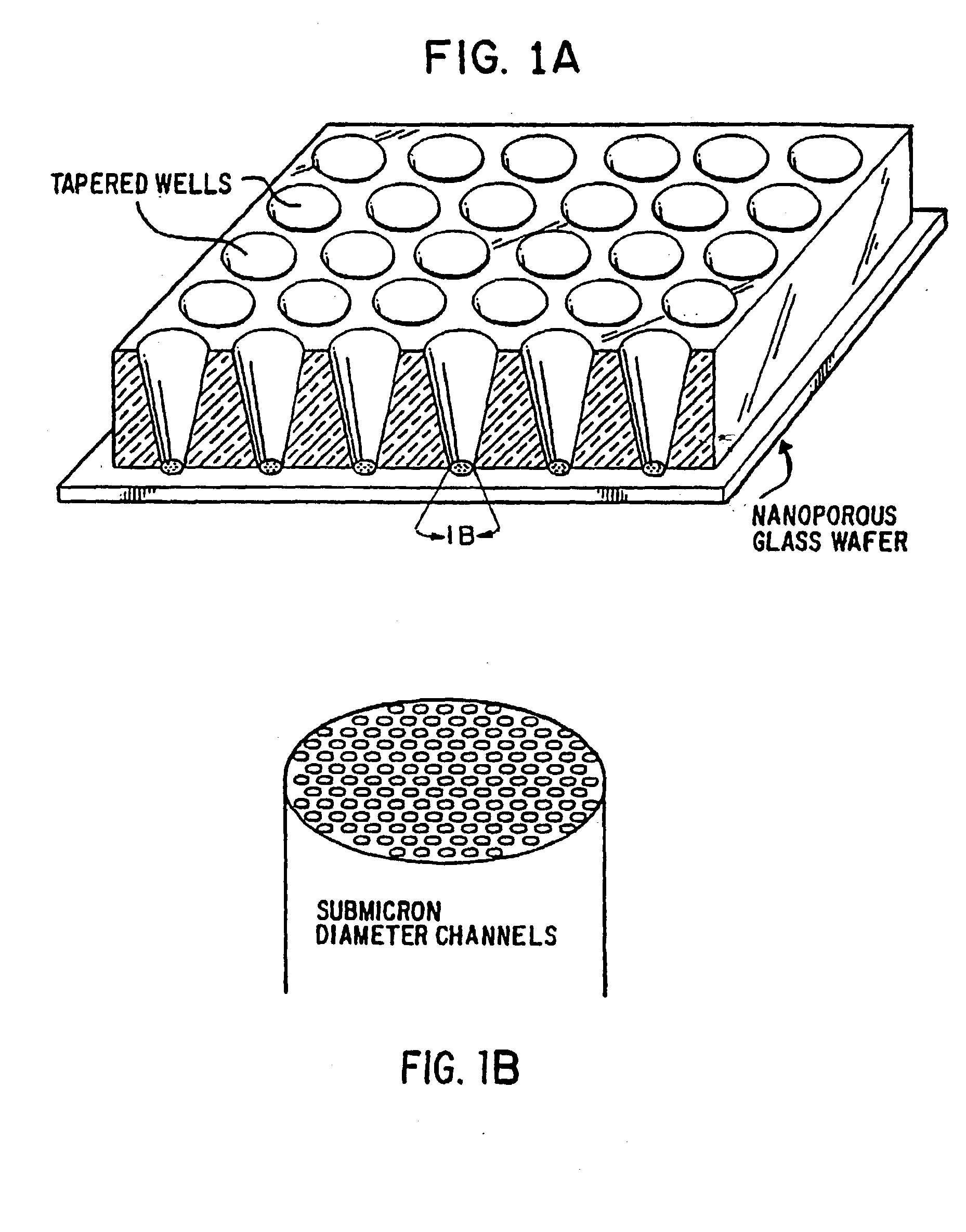
[0067] Nanochannel glass arrays developed at the Naval Research Laboratory can be used in the present invention to provide a high surface area nanochannel substrate to tether binding reagents such as DNA targets or probes for hybridization. NCG materials are glass structures containing a regular geometric array of parallel holes or channels as small as 33 nm in diameter or as large as a hundred micrometers or more in diameter. See Tonucci et al., Science 258: 783-785 (1992), and U.S. Pat. No. 5,234,594 which are incorporated herein by reference in their entireties. These nanochannel glass structures can be fabricated in various array configurations to provide a high surface area to volume ratio, and can possess packing densities in excess of 3×10¹⁰ channels per square centimeter. A variety of materials can be immobilized or fixed to the glass surfaces within the channels of the NCG array.
[0068] Nanochannel glass arrays are fabricated by arranging diss...
example 2
Silicon Wafers
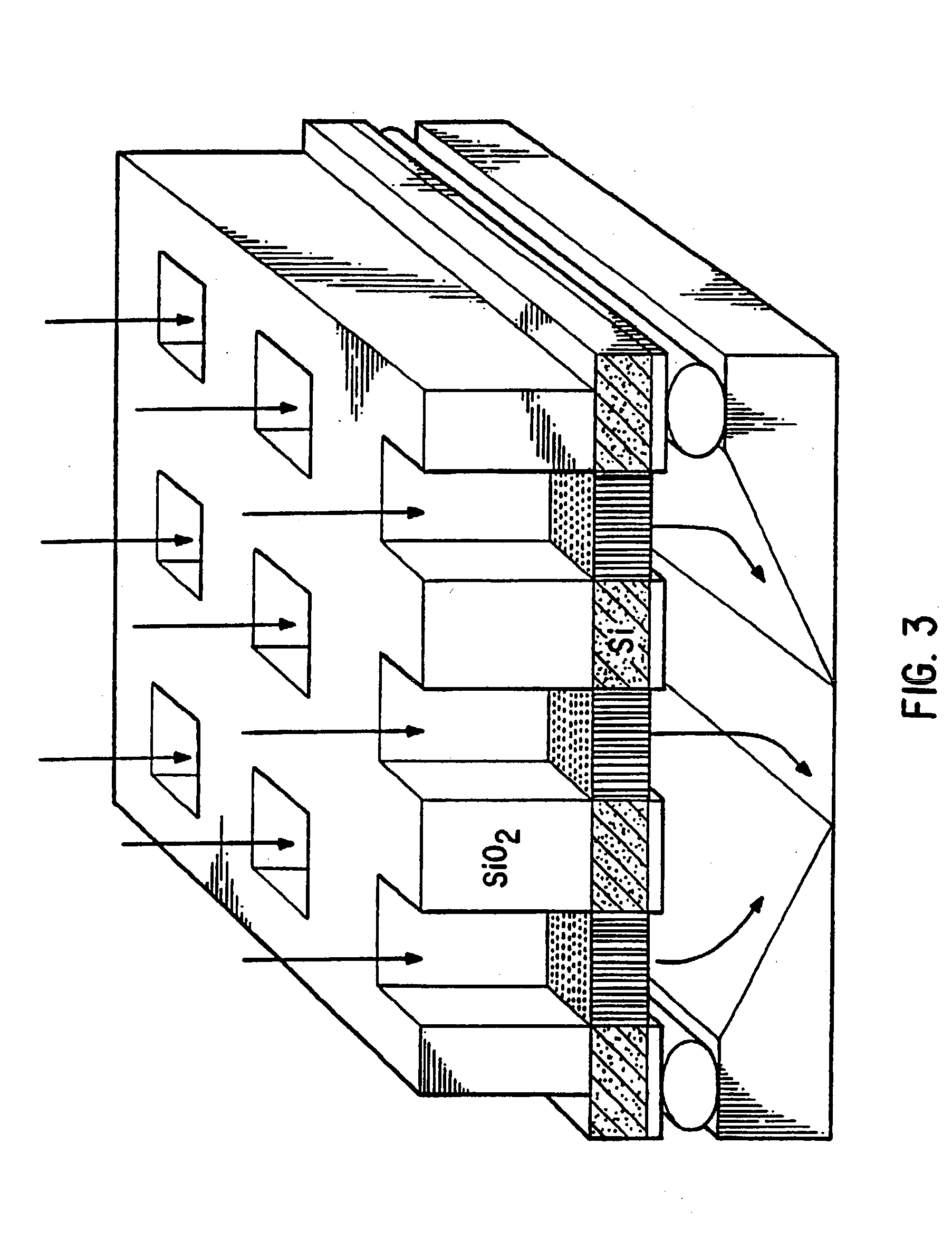
[0072] Two illustrative general types of silicon devices containing channels between a first and second surface of the device that can be prepared according to the process are described herein below.
[0073] Silicon designs containing channels are advantageously employed because of their adaptability to low cost mass production processes and their ability to incorporate in the fabrication process structural elements that function in fluidic entry and exit from the hybridization site and structures (e.g., electrodes) that may function in hybridization detection. Stable, open-cell materials containing channels between first and second surfaces of the material are used to accomplish enhancements and to introduce qualitatively new features in these devices, whereby the surface area of discrete and isolated binding regions comprising groups of channels is increased by a factor of 100 to 1000 relative to a two-dimensional surface.
[0074] Thin-film processing technology is us...
example 3
Well Arrays Defining Discrete and Isolated Binding Regions (Manifold)
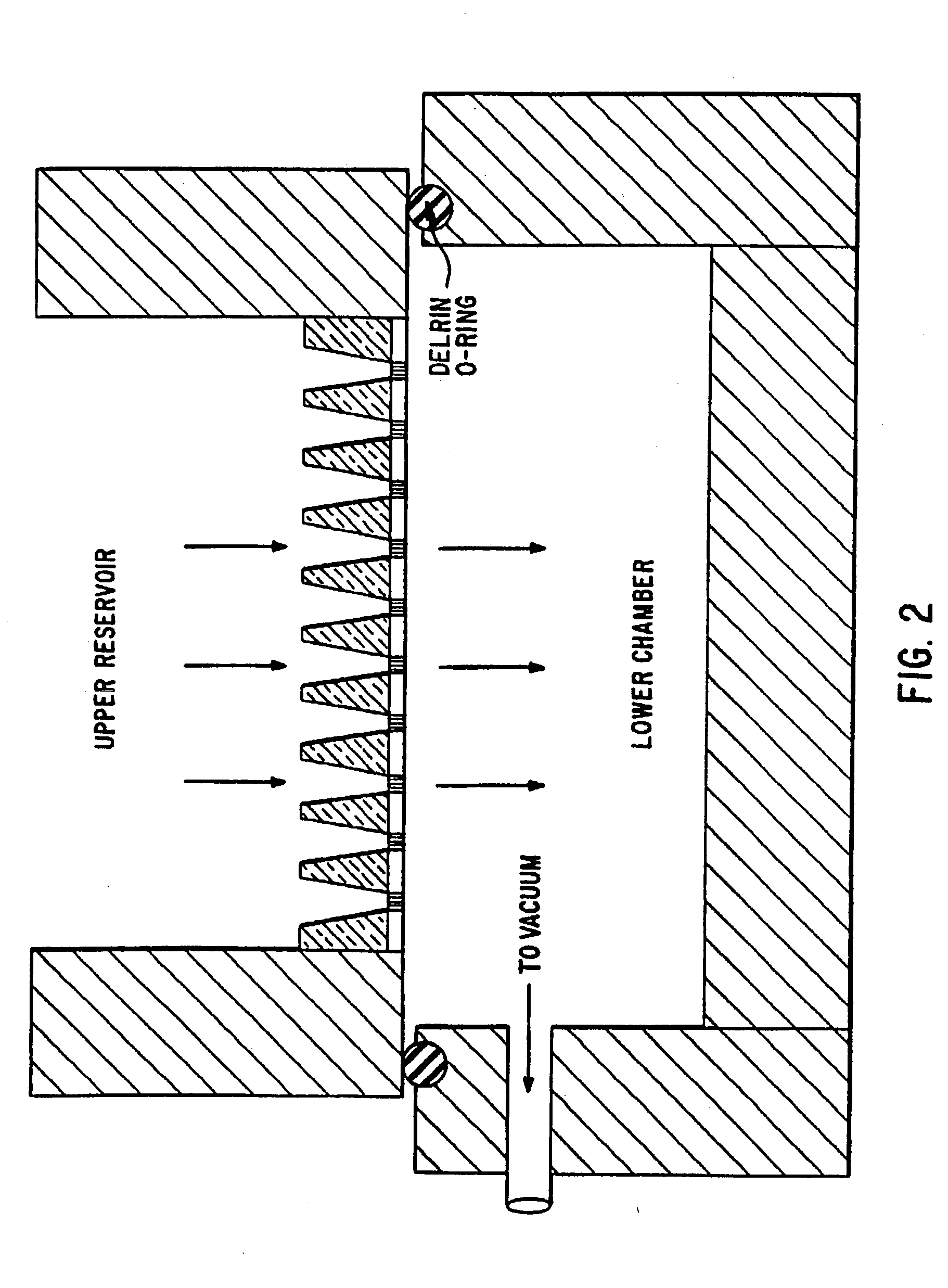
[0085] The NCG hybridization arrays described in Example 1 can be bonded to an array of orifices which align with the array of channels and serve as wells for placement of binding molecules, for instance, a substantially homogeneous sample of a biomolecule (e.g., a single DNA species) in defined sites (groups of channels) on the substrate. Such well arrays also can provide physical support and rigidity to the substrate such as a NCG wafer.
[0086] Polymeric well arrays can be fabricated using methods known in the art. For example, a polymeric layer suitable for use herein can be obtained from MicroFab Technologies, Inc., and the orifices can be fabricated using excimer laser machining. This method is preferred because existing technology is employed, allowing for low cost / high volume manufacturing.
[0087] Development of the polymeric array comprises: (1) materials selection; (2) ablation tooling and process develop...
PUM
| Property | Measurement | Unit |
|---|---|---|
| Thickness | aaaaa | aaaaa |
| Thickness | aaaaa | aaaaa |
| Diameter | aaaaa | aaaaa |
Abstract
Description
Claims
Application Information


