Eureka AIR delivers breakthrough ideas for toughest innovation challenges, trusted by R&D personnel around the world.

Photoconductor, image forming apparatus, image forming process, and process cartridge

a technology of photoconductor and image forming process, which is applied in the field of photoconductor, can solve the problems of titanyl phthalocyanine photoconductors that cannot establish both the higher speed and more compact size of the apparatus, and achieve the effect of stable image quality and high sensitivity

Active Publication Date: 2005-08-11
RICOH KK
View PDF4 Cites 71 Cited by
  • Summary
  • Abstract
  • Description
  • Claims
  • Application Information

AI Technical Summary

Benefits of technology

[0021] The object of the present invention is to provide a photoconductor that exhibits high sensitivity, stable image quality under repeated usages, and prolonged life, as well as a process cartridge, an image forming process, and an image forming apparatus that utilize the photoconductor respectively.
[0025] In accordance with the present invention, an electrophotographic photoconductor may be provided that shows high abrasion resistance under prolonged and repeated usages, and stably affords high quality images for a long term without causing abnormal images due to cracks, flaws, layer peels and the like derived from inferior cleaning, with controlling background smear as well as enhancing the potential stability.
[0027] The process cartridge according to the present invention may exhibit flaw resistance, abrasion resistance, and durability for a long term and may provide images with high quality owing to the photoconductor according to the present invention.
[0029] The image forming process according to the present invention may allow flaw resistance, abrasion resistance, and durability for a long term and may provide images with high quality owing to the photoconductor according to the present invention.
[0031] The image forming apparatus according to the present invention may afford flaw resistance, abrasion resistance, and durability for a long term and may provide images with high quality owing to the photoconductor according to the present invention.

Problems solved by technology

However, the photoconductors formed from the titanyl phthalocyanines are significantly susceptible to the background smear due to pigment flocculation or decreased charging property.
In particular, the background smear is a serious matter as described above.
Therefore, apparatuses with photoconductors formed from titanyl phthalocyanines are not establish both of the higher speed and more compacted size due to poor image stability, since the effect of the background smear is significant even if the higher speed is attained (see Japanese Patent Application Laid-Open (JP-A) No. 2001-19871).
Among these techniques, the use of a curable binder in (1) tends to cause reduction in image density since the curable binder has poor compatibility with the charge transporting material and impurities such as a polymerization initiator and unreacted residue is likely to increase the residual potential.
However, it is not sufficient for satisfying the durability required in the organic photoconductor.
Further, it is difficult to polymerize and purify the polymer charge transporting material.
Thus, it is impossible to obtain it at high purity and to attain stable electrical properties between materials upon using it.
In addition, it may cause problems such as high viscosity of the coating solution in terms of the preparation.
However, traps on the surface of the inorganic filler tends to increase the residual potential, thereby causing reduction in the image density.
Also, when unevenness of the inorganic filler and the binder resin on the surface of the photoconductor is severe, inferior cleaning may occur, resulting in toner peeling and image deletion.
With these techniques (1), (2) and (3), it is impossible to satisfy sufficiently the durability required for organic photoconductors, including electrical durability and mechanical durability.
Further, when a low molecular charge transport material is simply added to the surface layer, it may cause problems related with the compatibility to the cured body, thereby crystallization of the low molecular charge transporting material and clouding may occur, resulting in reduction in mechanical properties.
In addition, according to this photoconductor, since the monomer is reacted while it contains a polymer binder, the curing cannot be sufficiently progressed.
However, when a non-reactive resin is used as the binder resin, the binder resin is poorly compatible with the cured body produced by the reaction of the monomer and the charge transporting material, thereby surface unevenness during cross-linking forms from the phase separation, resulting in cleaning failure.
Also, as described above, in addition to the interference of the binder resin with the curing of the monomer, a bi-functional monomer which can be used in the photoconductor has a few functionality and fails to provide a sufficient cross-linkage density, thereby it is possible to obtain a sufficient abrasion resistance.
Also, when a reactive binder is used, since the number of functional groups contained in the monomer and the binder resin is small, the bonding of the charge transporting material and the cross-linkage density cannot be satisfied at the same time and the electrical properties and abrasion resistance are not sufficient.
However, according to the photoconductive layer, since the bulky transporting compound has two or more chain polymerizable functional groups, distortion may occur in the cured body, causing increase in internal stress, roughness of the surface layer, and formation of crack over the time.
Even in a photoconductor having a crosslinked photoconductive layer with a charge transporting structure attached in a chemical fashion, it cannot be said that general properties are sufficiently attained.
As explained above, even though the higher speed of apparatuses may be established through employing the photoconductors formed from titanyl phthalocyanines, the photoconductors must be often exchanged due to the decreased image quality caused by background smear; even though the abrasion resistance may be enhanced by forming a protective layer, the decrease of image quality may grow due to the increase of residual potential and inferior cleaning; as a result both of the higher sensitivity and prolonged life of the photoconductors desired for high-speed or color apparatuses have not been attained yet.

Method used


Image

  • Photoconductor, image forming apparatus, image forming process, and process cartridge
  • Photoconductor, image forming apparatus, image forming process, and process cartridge
  • Photoconductor, image forming apparatus, image forming process, and process cartridge

Examples


synthetic example 1

Charge Generating Substance

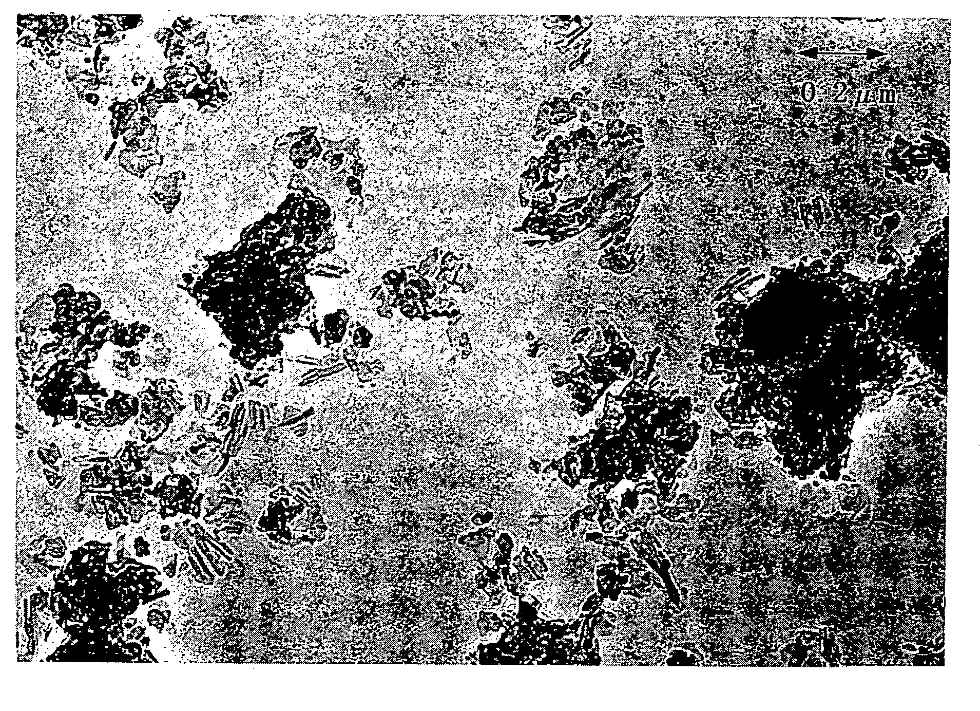
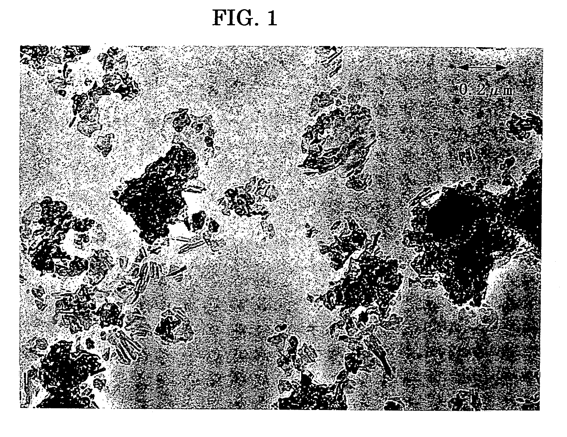
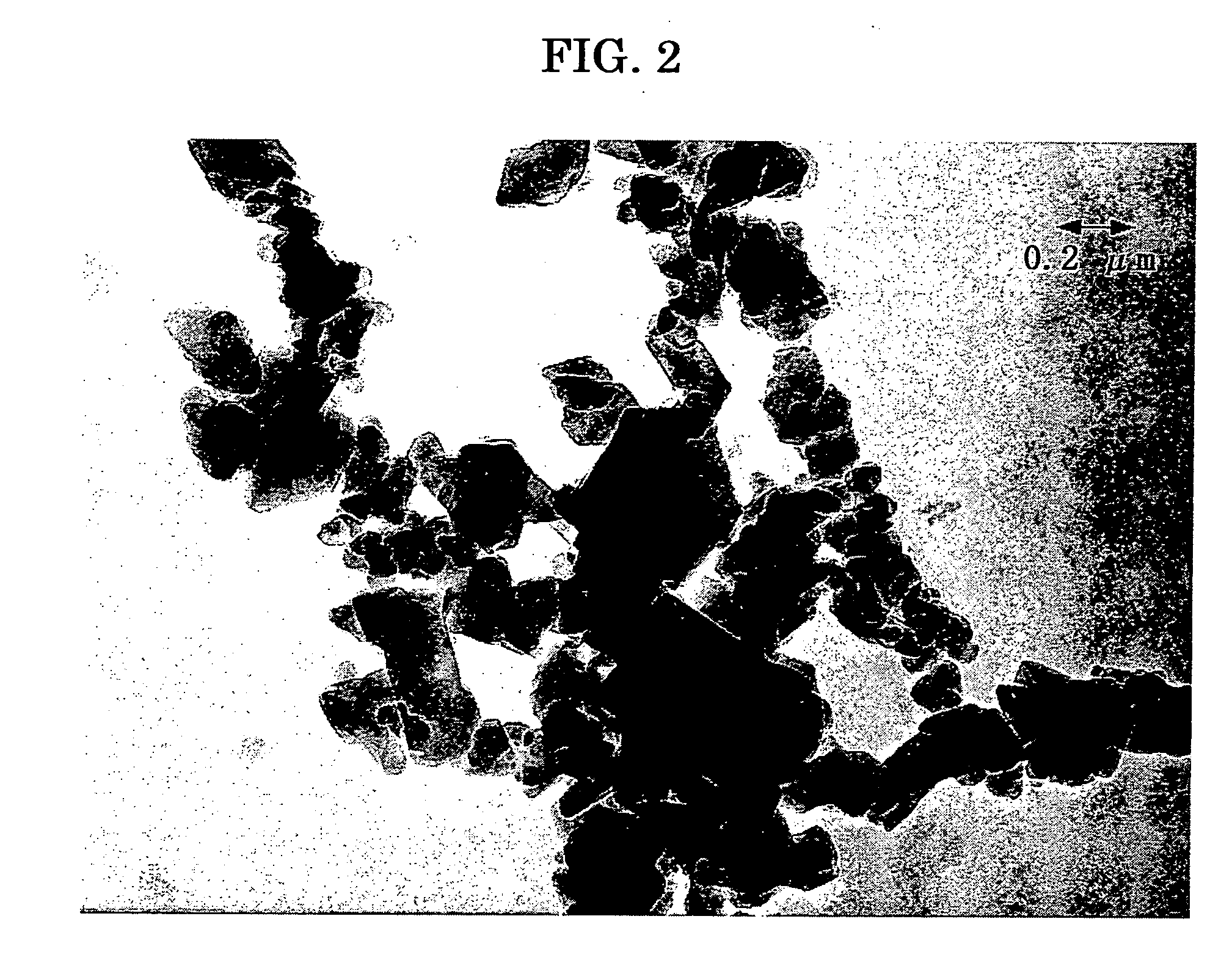
[0357] A titanyl phthalocyanine pigment was synthesized in a form of water paste in the similar Comparative Synthetic Example 1, the product was subjected to crystal transformation in accordance with the following way, to prepare a titanyl phthalocyanine crystal having smaller primary particle size than Comparative Synthetic Example 1.

[0358] To the 60 parts of water paste, obtained in Comparative Synthetic Example 1, prior to the crystal transformation, 400 parts of tetrahydrofuran was added and was stirred vigorously at 2000 rpm by means of Homomixer (Model Mark IIf, by Kenis). The stirring was stopped when the color of the paste turned from dark blue to light blue after 20 minutes from starting the stirring, immediately then the filtering was conducted under a reduced pressure. The crystal obtained on the filter was rinsed with tetrahydrofuran to obtain a wet cake of pigment.

[0359] The wet cake was dried at 70° C. under a reduced pressure of 5 mm Hg f...

preparation example 1

Dispersion

[0374] The pigment 1, prepared in Comparative Synthetic Example 1, was dispersed in the following conditions to prepare a dispersion of coating liquid for charge generating layer.

Pigment of titanyl phthalocyanine (Pigment 1) 15 partsPolyvinyl butyral (BX-1, Sekisui Chemical Co.) 10 parts2-butanone280 parts

[0375] Using a commercially available dispersing apparatus of beads mill type and PSZ balls of 0.5 mm in diameter, the pigment, polyvinyl butyral, and 2-butanone was poured into the dispersing apparatus, and subjected to dispersing for 30 minutes at 1200 rpm of rotor rotating number to prepare a dispersion, which is referred to as dispersion 1.

preparation examples 2 to 9

Dispersion

[0376] Dispersions were prepared in the same manner as Preparation Example 1, except for changing the pigment 1 into the pigments 2 to 9 obtained in Comparative Synthetic Example 2 to 8 and Synthetic Example 1, which are referred to as dispersions 2 to 9 corresponding to the number of pigments.


PUM


Abstract

The object of the present invention is to provide a photoconductor that is highly sensitive, stable in image quality under repeated usages, and affords prolonged life. In order attain the object, a photoconductor is provided that comprises a charge generating layer, a charge transporting layer, and a crosslinked charge transporting layer, on an substrate in order, the charge generating layer contains titanyl phthalocyanine crystal particles that exhibit a highest peak at 27.2°, main peaks at 9.4°, 9.6° and 24.0°, a peak at 7.3° as the lowest angle, and with no peaks in a range between 7.3° and 9.4°, and with no peak at 26.3° as Bragg 2θangles (±0.2°) in terms of CuK-α characteristic X-ray wavelength at 1.542 Å, and the averaged primary particle size of the titanyl phthalocyanine crystal particles is 0.25 μm or less, and the crosslinked charge transporting layer contains a reaction product of a radical polymerizable monomer having three or more functionalities and no charge transporting structure and a radical polymerizable compound having one functionality and a charge transporting structure, and the thickness of the crosslinked charge transporting layer is 1 to 10 μm.

Description

BACKGROUND OF THE INVENTION [0001] 1. Field of the Invention [0002] The present invention relates to a photoconductor that comprises a photoconductive layer, wherein the photoconductive layer comprises a charge generating layer, a charge transporting layer, and a crosslinked charge transporting layer, and wherein these layers are laminated in order on a substrate; and a image forming process, a image forming apparatus, and a process cartridge that utilize the photoconductor respectively. [0003] 2. Description of the Related Art [0004] Information processing systems based on electrophotographic process have been dramatically developing. In particular, laser printers and digital copiers, which convert information into digital signals and record the information through optical technologies, have been remarkably improved in their printing quality and reliability. These laser printers and digital copiers are still demanded higher image quality, higher speed, and more compacted size. [000...

Claims


Application Information

Patent Timeline
Patent Type & Authority Applications(United States)
IPC IPC(8): G03G5/047G03G5/05G03G5/06G03G5/07G03G15/02
CPCG03G5/0546G03G5/0589G03G5/071G03G5/0696G03G5/0592G03G5/072G03G5/0732G03G5/074G03G5/0745
Inventor TAMOTO, NOZOMUNIIMI, TATSUYASUZUKI, TETSUROOHTA, KATSUICHI
Owner RICOH KK
Why Eureka
Eureka Blog
Learn More